 | –≠–ª–µ–∫—Ç—Ä–æ–Ω–Ω—ã–π –∫–æ–º–ø–æ–Ω–µ–Ω—Ç: ST62E01C | –°–∫–∞—á–∞—Ç—å:  PDF PDF  ZIP ZIP |
Rev. 3.2
July 2001
1/100
ST6200C/ST6201C/ST6203C
8-BIT MCUs WITH A/D CONVERTER,
TWO TIMERS, OSCILLATOR SAFEGUARD & SAFE RESET
s
Memories
≠ 1K or 2K bytes Program memory (OTP,
EPROM, FASTROM or ROM) with read-out
protection
≠ 64 bytes RAM
s
Clock, Reset and Supply Management
≠ Enhanced reset system
≠ Low Voltage Detector (LVD) for Safe Reset
≠ Clock sources: crystal/ceramic resonator or
RC network, external clock, backup oscillator
(LFAO)
≠ Oscillator Safeguard (OSG)
≠ 2 Power Saving Modes: Wait and Stop
s
Interrupt Management
≠ 4 interrupt vectors plus NMI and RESET
≠ 9 external interrupt lines (on 2 vectors)
s
9 I/O Ports
≠ 9 multifunctional bidirectional I/O lines
≠ 4 alternate function lines
≠ 3 high sink outputs (20mA)
s
2 Timers
≠ Configurable watchdog timer
≠ 8-bit timer/counter with a 7-bit prescaler
s
Analog Peripheral
≠ 8-bit ADC with 4 input channels (except on
ST6203C)
s
Instruction Set
≠ 8-bit data manipulation
≠ 40 basic instructions
≠ 9 addressing modes
≠ Bit manipulation
s
Development Tools
≠ Full hardware/software development package
Device Summary
(See
Section 11.5
for Ordering Information)
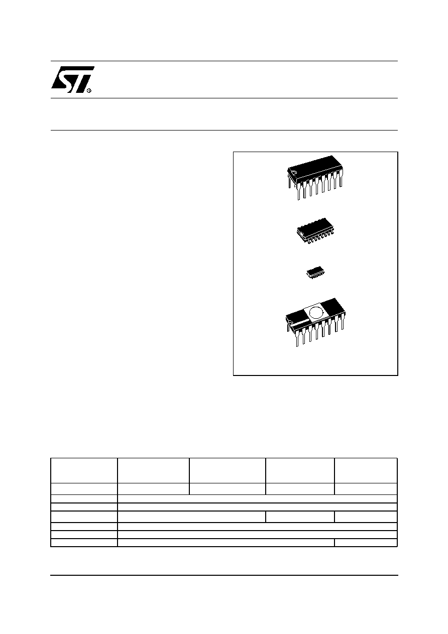
PDIP16
SO16
CDIP16W
SSOP16
Features
ST62T00C(OTP)
ST6200C(ROM)
ST62P00C(FASTROM)
ST62T01C(OTP)
ST6201C(ROM)
ST62P01C(FASTROM)
ST62T03C(OTP)
ST6203C(ROM)
ST62P03C(FASTROM)
ST62E01C(EPROM)
Program memory - bytes
1K
2K
1K
2K
RAM - bytes
64
Operating Supply
3.0V to 6V
Analog Inputs
4
-
4
Clock Frequency
8MHz Max
Operating Temperature
-40∞C to +125∞C
Packages
PDIP16 / SO16 / SSOP16
CDIP16W
1

Table of Contents
100
2/100
2
ST6200C/ST6201C/ST6203C . . . . . . . . . . . . . . . . . . . . . . . . . . . 1
1 INTRODUCTION . . . . . . . . . . . . . . . . . . . . . . . . . . . . . . . . . . . . . . . . . . . . . . . . . . . . . . . . . . . . . . 6
2 PIN DESCRIPTION . . . . . . . . . . . . . . . . . . . . . . . . . . . . . . . . . . . . . . . . . . . . . . . . . . . . . . . . . . . . 7
3 MEMORY MAPS, PROGRAMMING MODES AND OPTION BYTES . . . . . . . . . . . . . . . . . . . . . . 8
3.1
MEMORY AND REGISTER MAPS . . . . . . . . . . . . . . . . . . . . . . . . . . . . . . . . . . . . . . . . . . 8
3.1.1 Introduction . . . . . . . . . . . . . . . . . . . . . . . . . . . . . . . . . . . . . . . . . . . . . . . . . . . . . . . . 8
3.1.2 Program Space . . . . . . . . . . . . . . . . . . . . . . . . . . . . . . . . . . . . . . . . . . . . . . . . . . . . 10
3.1.3 Readout Protection . . . . . . . . . . . . . . . . . . . . . . . . . . . . . . . . . . . . . . . . . . . . . . . . . 10
3.1.4 Data Space . . . . . . . . . . . . . . . . . . . . . . . . . . . . . . . . . . . . . . . . . . . . . . . . . . . . . . . 10
3.1.5 Stack Space . . . . . . . . . . . . . . . . . . . . . . . . . . . . . . . . . . . . . . . . . . . . . . . . . . . . . . . 10
3.1.6 Data ROM Window . . . . . . . . . . . . . . . . . . . . . . . . . . . . . . . . . . . . . . . . . . . . . . . . . 12
3.2
PROGRAMMING MODES . . . . . . . . . . . . . . . . . . . . . . . . . . . . . . . . . . . . . . . . . . . . . . . . 14
3.2.1 Program Memory . . . . . . . . . . . . . . . . . . . . . . . . . . . . . . . . . . . . . . . . . . . . . . . . . . . 14
3.2.2 EPROM Erasing . . . . . . . . . . . . . . . . . . . . . . . . . . . . . . . . . . . . . . . . . . . . . . . . . . . . 14
3.3
OPTION BYTES . . . . . . . . . . . . . . . . . . . . . . . . . . . . . . . . . . . . . . . . . . . . . . . . . . . . . . . 15
4 CENTRAL PROCESSING UNIT . . . . . . . . . . . . . . . . . . . . . . . . . . . . . . . . . . . . . . . . . . . . . . . . . 16
4.1
INTRODUCTION . . . . . . . . . . . . . . . . . . . . . . . . . . . . . . . . . . . . . . . . . . . . . . . . . . . . . . . 16
4.2
MAIN FEATURES . . . . . . . . . . . . . . . . . . . . . . . . . . . . . . . . . . . . . . . . . . . . . . . . . . . . . . 16
4.3
CPU REGISTERS . . . . . . . . . . . . . . . . . . . . . . . . . . . . . . . . . . . . . . . . . . . . . . . . . . . . . . 16
5 CLOCKS, SUPPLY AND RESET . . . . . . . . . . . . . . . . . . . . . . . . . . . . . . . . . . . . . . . . . . . . . . . . 18
5.1
CLOCK SYSTEM . . . . . . . . . . . . . . . . . . . . . . . . . . . . . . . . . . . . . . . . . . . . . . . . . . . . . . . 18
5.1.1 Main Oscillator . . . . . . . . . . . . . . . . . . . . . . . . . . . . . . . . . . . . . . . . . . . . . . . . . . . . . 19
5.1.2 Oscillator Safeguard (OSG) . . . . . . . . . . . . . . . . . . . . . . . . . . . . . . . . . . . . . . . . . . . 20
5.1.3 Low Frequency Auxiliary Oscillator (LFAO) . . . . . . . . . . . . . . . . . . . . . . . . . . . . . . . 21
5.1.4 Register Description . . . . . . . . . . . . . . . . . . . . . . . . . . . . . . . . . . . . . . . . . . . . . . . . . 21
5.2
LOW VOLTAGE DETECTOR (LVD) . . . . . . . . . . . . . . . . . . . . . . . . . . . . . . . . . . . . . . . . 22
5.3
RESET . . . . . . . . . . . . . . . . . . . . . . . . . . . . . . . . . . . . . . . . . . . . . . . . . . . . . . . . . . . . . . . 23
5.3.1 Introduction . . . . . . . . . . . . . . . . . . . . . . . . . . . . . . . . . . . . . . . . . . . . . . . . . . . . . . . 23
5.3.2 RESET Sequence . . . . . . . . . . . . . . . . . . . . . . . . . . . . . . . . . . . . . . . . . . . . . . . . . . 23
5.3.3 RESET Pin . . . . . . . . . . . . . . . . . . . . . . . . . . . . . . . . . . . . . . . . . . . . . . . . . . . . . . . . 24
5.3.4 Watchdog Reset . . . . . . . . . . . . . . . . . . . . . . . . . . . . . . . . . . . . . . . . . . . . . . . . . . . 25
5.3.5 LVD Reset . . . . . . . . . . . . . . . . . . . . . . . . . . . . . . . . . . . . . . . . . . . . . . . . . . . . . . . . 25
5.4
INTERRUPTS . . . . . . . . . . . . . . . . . . . . . . . . . . . . . . . . . . . . . . . . . . . . . . . . . . . . . . . . . 26
5.5
INTERRUPT RULES AND PRIORITY MANAGEMENT . . . . . . . . . . . . . . . . . . . . . . . . . 27
5.6
INTERRUPTS AND LOW POWER MODES . . . . . . . . . . . . . . . . . . . . . . . . . . . . . . . . . . 27
5.7
NON MASKABLE INTERRUPT . . . . . . . . . . . . . . . . . . . . . . . . . . . . . . . . . . . . . . . . . . . . 27
5.8
PERIPHERAL INTERRUPTS . . . . . . . . . . . . . . . . . . . . . . . . . . . . . . . . . . . . . . . . . . . . . 27
5.9
EXTERNAL INTERRUPTS (I/O PORTS) . . . . . . . . . . . . . . . . . . . . . . . . . . . . . . . . . . . . 28
5.9.1 Notes on using External Interrupts . . . . . . . . . . . . . . . . . . . . . . . . . . . . . . . . . . . . . . 28
5.10 INTERRUPT HANDLING PROCEDURE . . . . . . . . . . . . . . . . . . . . . . . . . . . . . . . . . . . . . 29
5.10.1Interrupt Response Time . . . . . . . . . . . . . . . . . . . . . . . . . . . . . . . . . . . . . . . . . . . . . 29
5.11 REGISTER DESCRIPTION . . . . . . . . . . . . . . . . . . . . . . . . . . . . . . . . . . . . . . . . . . . . . . . 30

Table of Contents
3/100
3
6 POWER SAVING MODES . . . . . . . . . . . . . . . . . . . . . . . . . . . . . . . . . . . . . . . . . . . . . . . . . . . . . 31
6.1
INTRODUCTION . . . . . . . . . . . . . . . . . . . . . . . . . . . . . . . . . . . . . . . . . . . . . . . . . . . . . . . 31
6.2
WAIT MODE . . . . . . . . . . . . . . . . . . . . . . . . . . . . . . . . . . . . . . . . . . . . . . . . . . . . . . . . . . 32
6.3
STOP MODE . . . . . . . . . . . . . . . . . . . . . . . . . . . . . . . . . . . . . . . . . . . . . . . . . . . . . . . . . . 33
6.4
NOTES RELATED TO WAIT AND STOP MODES . . . . . . . . . . . . . . . . . . . . . . . . . . . . . 35
6.4.1 Exit from Wait and Stop Modes . . . . . . . . . . . . . . . . . . . . . . . . . . . . . . . . . . . . . . . . 35
6.4.2 Recommended MCU Configuration . . . . . . . . . . . . . . . . . . . . . . . . . . . . . . . . . . . . . 35
7 I/O PORTS . . . . . . . . . . . . . . . . . . . . . . . . . . . . . . . . . . . . . . . . . . . . . . . . . . . . . . . . . . . . . . . . . . 36
7.1
INTRODUCTION . . . . . . . . . . . . . . . . . . . . . . . . . . . . . . . . . . . . . . . . . . . . . . . . . . . . . . . 36
7.2
FUNCTIONAL DESCRIPTION . . . . . . . . . . . . . . . . . . . . . . . . . . . . . . . . . . . . . . . . . . . . 36
7.2.1 Digital Input Modes . . . . . . . . . . . . . . . . . . . . . . . . . . . . . . . . . . . . . . . . . . . . . . . . . 36
7.2.2 Analog Inputs . . . . . . . . . . . . . . . . . . . . . . . . . . . . . . . . . . . . . . . . . . . . . . . . . . . . . . 36
7.2.3 Output Modes . . . . . . . . . . . . . . . . . . . . . . . . . . . . . . . . . . . . . . . . . . . . . . . . . . . . . 36
7.2.4 Alternate Functions . . . . . . . . . . . . . . . . . . . . . . . . . . . . . . . . . . . . . . . . . . . . . . . . . 36
7.2.5 Instructions NOT to be used to access Port Data registers (SET, RES, INC and DEC)
. . . . . . . . . . . . . . . . . . . . . . . . . . . . . . . . . . . . . . . . . . . . . . . . . . . . . . . . . . . . . . . . . 38
7.2.6 Recommendations . . . . . . . . . . . . . . . . . . . . . . . . . . . . . . . . . . . . . . . . . . . . . . . . . . 38
7.3
LOW POWER MODES . . . . . . . . . . . . . . . . . . . . . . . . . . . . . . . . . . . . . . . . . . . . . . . . . . 38
7.4
INTERRUPTS . . . . . . . . . . . . . . . . . . . . . . . . . . . . . . . . . . . . . . . . . . . . . . . . . . . . . . . . . 38
7.5
REGISTER DESCRIPTION . . . . . . . . . . . . . . . . . . . . . . . . . . . . . . . . . . . . . . . . . . . . . . . 40
8 ON-CHIP PERIPHERALS . . . . . . . . . . . . . . . . . . . . . . . . . . . . . . . . . . . . . . . . . . . . . . . . . . . . . . 41
8.1
WATCHDOG TIMER (WDG) . . . . . . . . . . . . . . . . . . . . . . . . . . . . . . . . . . . . . . . . . . . . . . 41
8.1.1 Introduction . . . . . . . . . . . . . . . . . . . . . . . . . . . . . . . . . . . . . . . . . . . . . . . . . . . . . . . 41
8.1.2 Main Features . . . . . . . . . . . . . . . . . . . . . . . . . . . . . . . . . . . . . . . . . . . . . . . . . . . . . 41
8.1.3 Functional Description . . . . . . . . . . . . . . . . . . . . . . . . . . . . . . . . . . . . . . . . . . . . . . . 42
8.1.4 Recommendations . . . . . . . . . . . . . . . . . . . . . . . . . . . . . . . . . . . . . . . . . . . . . . . . . . 42
8.1.5 Low Power Modes . . . . . . . . . . . . . . . . . . . . . . . . . . . . . . . . . . . . . . . . . . . . . . . . . . 43
8.1.6 Interrupts . . . . . . . . . . . . . . . . . . . . . . . . . . . . . . . . . . . . . . . . . . . . . . . . . . . . . . . . . 43
8.1.7 Register Description . . . . . . . . . . . . . . . . . . . . . . . . . . . . . . . . . . . . . . . . . . . . . . . . . 44
8.2
8-BIT TIMER . . . . . . . . . . . . . . . . . . . . . . . . . . . . . . . . . . . . . . . . . . . . . . . . . . . . . . . . . . 45
8.2.1 Introduction . . . . . . . . . . . . . . . . . . . . . . . . . . . . . . . . . . . . . . . . . . . . . . . . . . . . . . . 45
8.2.2 Main Features . . . . . . . . . . . . . . . . . . . . . . . . . . . . . . . . . . . . . . . . . . . . . . . . . . . . . 45
8.2.3 Counter/Prescaler Description . . . . . . . . . . . . . . . . . . . . . . . . . . . . . . . . . . . . . . . . . 46
8.2.4 Low Power Modes . . . . . . . . . . . . . . . . . . . . . . . . . . . . . . . . . . . . . . . . . . . . . . . . . . 46
8.2.5 Interrupts . . . . . . . . . . . . . . . . . . . . . . . . . . . . . . . . . . . . . . . . . . . . . . . . . . . . . . . . . 46
8.2.6 Register Description . . . . . . . . . . . . . . . . . . . . . . . . . . . . . . . . . . . . . . . . . . . . . . . . . 47
8.3
A/D CONVERTER (ADC) . . . . . . . . . . . . . . . . . . . . . . . . . . . . . . . . . . . . . . . . . . . . . . . . 48
8.3.1 Introduction . . . . . . . . . . . . . . . . . . . . . . . . . . . . . . . . . . . . . . . . . . . . . . . . . . . . . . . 48
8.3.2 Main Features . . . . . . . . . . . . . . . . . . . . . . . . . . . . . . . . . . . . . . . . . . . . . . . . . . . . . 48
8.3.3 Functional Description . . . . . . . . . . . . . . . . . . . . . . . . . . . . . . . . . . . . . . . . . . . . . . . 49
8.3.4 Recommendations . . . . . . . . . . . . . . . . . . . . . . . . . . . . . . . . . . . . . . . . . . . . . . . . . . 50
8.3.5 Low Power Modes . . . . . . . . . . . . . . . . . . . . . . . . . . . . . . . . . . . . . . . . . . . . . . . . . . 51
8.3.6 Interrupts . . . . . . . . . . . . . . . . . . . . . . . . . . . . . . . . . . . . . . . . . . . . . . . . . . . . . . . . . 51
8.3.7 Register Description . . . . . . . . . . . . . . . . . . . . . . . . . . . . . . . . . . . . . . . . . . . . . . . . . 51

Table of Contents
100
4/100
9 INSTRUCTION SET . . . . . . . . . . . . . . . . . . . . . . . . . . . . . . . . . . . . . . . . . . . . . . . . . . . . . . . . . . 52
9.1
ST6 ARCHITECTURE . . . . . . . . . . . . . . . . . . . . . . . . . . . . . . . . . . . . . . . . . . . . . . . . . . . 52
9.2
ADDRESSING MODES . . . . . . . . . . . . . . . . . . . . . . . . . . . . . . . . . . . . . . . . . . . . . . . . . . 52
9.3
INSTRUCTION SET . . . . . . . . . . . . . . . . . . . . . . . . . . . . . . . . . . . . . . . . . . . . . . . . . . . . 53
10 ELECTRICAL CHARACTERISTICS . . . . . . . . . . . . . . . . . . . . . . . . . . . . . . . . . . . . . . . . . . . . . 58
10.1 PARAMETER CONDITIONS . . . . . . . . . . . . . . . . . . . . . . . . . . . . . . . . . . . . . . . . . . . . . . 58
10.1.1Minimum and Maximum Values . . . . . . . . . . . . . . . . . . . . . . . . . . . . . . . . . . . . . . . . 58
10.1.2Typical Values . . . . . . . . . . . . . . . . . . . . . . . . . . . . . . . . . . . . . . . . . . . . . . . . . . . . . 58
10.1.3Typical Curves . . . . . . . . . . . . . . . . . . . . . . . . . . . . . . . . . . . . . . . . . . . . . . . . . . . . . 58
10.1.4Loading Capacitor . . . . . . . . . . . . . . . . . . . . . . . . . . . . . . . . . . . . . . . . . . . . . . . . . . 58
10.1.5Pin Input Voltage . . . . . . . . . . . . . . . . . . . . . . . . . . . . . . . . . . . . . . . . . . . . . . . . . . . 58
10.2 ABSOLUTE MAXIMUM RATINGS . . . . . . . . . . . . . . . . . . . . . . . . . . . . . . . . . . . . . . . . . 59
10.2.1Voltage Characteristics . . . . . . . . . . . . . . . . . . . . . . . . . . . . . . . . . . . . . . . . . . . . . . 59
10.2.2Current Characteristics . . . . . . . . . . . . . . . . . . . . . . . . . . . . . . . . . . . . . . . . . . . . . . 59
10.2.3Thermal Characteristics . . . . . . . . . . . . . . . . . . . . . . . . . . . . . . . . . . . . . . . . . . . . . 59
10.3 OPERATING CONDITIONS . . . . . . . . . . . . . . . . . . . . . . . . . . . . . . . . . . . . . . . . . . . . . . 60
10.3.1General Operating Conditions . . . . . . . . . . . . . . . . . . . . . . . . . . . . . . . . . . . . . . . . 60
10.3.2Operating Conditions with Low Voltage Detector (LVD) . . . . . . . . . . . . . . . . . . . . . 61
10.4 SUPPLY CURRENT CHARACTERISTICS . . . . . . . . . . . . . . . . . . . . . . . . . . . . . . . . . . . 62
10.4.1RUN Modes . . . . . . . . . . . . . . . . . . . . . . . . . . . . . . . . . . . . . . . . . . . . . . . . . . . . . . 62
10.4.2WAIT Modes . . . . . . . . . . . . . . . . . . . . . . . . . . . . . . . . . . . . . . . . . . . . . . . . . . . . . . 63
10.4.3STOP Mode . . . . . . . . . . . . . . . . . . . . . . . . . . . . . . . . . . . . . . . . . . . . . . . . . . . . . . 66
10.4.4Supply and Clock System . . . . . . . . . . . . . . . . . . . . . . . . . . . . . . . . . . . . . . . . . . . . 67
10.4.5On-Chip Peripherals . . . . . . . . . . . . . . . . . . . . . . . . . . . . . . . . . . . . . . . . . . . . . . . . 67
10.5 CLOCK AND TIMING CHARACTERISTICS . . . . . . . . . . . . . . . . . . . . . . . . . . . . . . . . . . 68
10.5.1General Timings . . . . . . . . . . . . . . . . . . . . . . . . . . . . . . . . . . . . . . . . . . . . . . . . . . . 68
10.5.2External Clock Source . . . . . . . . . . . . . . . . . . . . . . . . . . . . . . . . . . . . . . . . . . . . . . . 68
10.5.3Crystal and Ceramic Resonator Oscillators . . . . . . . . . . . . . . . . . . . . . . . . . . . . . . . 69
10.5.4RC Oscillator . . . . . . . . . . . . . . . . . . . . . . . . . . . . . . . . . . . . . . . . . . . . . . . . . . . . . . 70
10.5.5Oscillator Safeguard (OSG) and Low Frequency Auxiliary Oscillator (LFAO) . . . . . 71
10.6 MEMORY CHARACTERISTICS . . . . . . . . . . . . . . . . . . . . . . . . . . . . . . . . . . . . . . . . . . . 72
10.6.1RAM and Hardware Registers . . . . . . . . . . . . . . . . . . . . . . . . . . . . . . . . . . . . . . . . 72
10.6.2EPROM Program Memory . . . . . . . . . . . . . . . . . . . . . . . . . . . . . . . . . . . . . . . . . . . 72
10.7 EMC CHARACTERISTICS . . . . . . . . . . . . . . . . . . . . . . . . . . . . . . . . . . . . . . . . . . . . . . . 73
10.7.1Functional EMS . . . . . . . . . . . . . . . . . . . . . . . . . . . . . . . . . . . . . . . . . . . . . . . . . . . . 73
10.7.2Absolute Electrical Sensitivity . . . . . . . . . . . . . . . . . . . . . . . . . . . . . . . . . . . . . . . . . 74
10.7.3ESD Pin Protection Strategy . . . . . . . . . . . . . . . . . . . . . . . . . . . . . . . . . . . . . . . . . . 76
10.8 I/O PORT PIN CHARACTERISTICS . . . . . . . . . . . . . . . . . . . . . . . . . . . . . . . . . . . . . . . . 77
10.8.1General Characteristics . . . . . . . . . . . . . . . . . . . . . . . . . . . . . . . . . . . . . . . . . . . . . . 77
10.8.2Output Driving Current . . . . . . . . . . . . . . . . . . . . . . . . . . . . . . . . . . . . . . . . . . . . . . . 78
10.9 CONTROL PIN CHARACTERISTICS . . . . . . . . . . . . . . . . . . . . . . . . . . . . . . . . . . . . . . . 81
10.9.1Asynchronous RESET Pin . . . . . . . . . . . . . . . . . . . . . . . . . . . . . . . . . . . . . . . . . . . . 81
10.9.2NMI Pin . . . . . . . . . . . . . . . . . . . . . . . . . . . . . . . . . . . . . . . . . . . . . . . . . . . . . . . . . . 82
10.10 TIMER PERIPHERAL CHARACTERISTICS . . . . . . . . . . . . . . . . . . . . . . . . . . . . . . . . . . 83
10.10.1Watchdog Timer . . . . . . . . . . . . . . . . . . . . . . . . . . . . . . . . . . . . . . . . . . . . . . . . . . 83
10.10.28-Bit Timer . . . . . . . . . . . . . . . . . . . . . . . . . . . . . . . . . . . . . . . . . . . . . . . . . . . . . . . 83
1

Table of Contents
5/100
10.11 8-BIT ADC CHARACTERISTICS . . . . . . . . . . . . . . . . . . . . . . . . . . . . . . . . . . . . . . . . . . 84
11 GENERAL INFORMATION . . . . . . . . . . . . . . . . . . . . . . . . . . . . . . . . . . . . . . . . . . . . . . . . . . . . 86
11.1 PACKAGE MECHANICAL DATA . . . . . . . . . . . . . . . . . . . . . . . . . . . . . . . . . . . . . . . . . . 86
11.2 THERMAL CHARACTERISTICS . . . . . . . . . . . . . . . . . . . . . . . . . . . . . . . . . . . . . . . . . . 88
11.3 SOLDERING AND GLUEABILITY INFORMATION . . . . . . . . . . . . . . . . . . . . . . . . . . . . . 89
11.4 PACKAGE/SOCKET FOOTPRINT PROPOSAL . . . . . . . . . . . . . . . . . . . . . . . . . . . . . . . 90
11.5 ORDERING INFORMATION . . . . . . . . . . . . . . . . . . . . . . . . . . . . . . . . . . . . . . . . . . . . . . 91
11.6 TRANSFER OF CUSTOMER CODE . . . . . . . . . . . . . . . . . . . . . . . . . . . . . . . . . . . . . . . 92
11.6.1FASTROM version . . . . . . . . . . . . . . . . . . . . . . . . . . . . . . . . . . . . . . . . . . . . . . . . . . 92
11.6.2ROM VERSION . . . . . . . . . . . . . . . . . . . . . . . . . . . . . . . . . . . . . . . . . . . . . . . . . . . . 93
12 DEVELOPMENT TOOLS . . . . . . . . . . . . . . . . . . . . . . . . . . . . . . . . . . . . . . . . . . . . . . . . . . . . . 95
13 ST6 APPLICATION NOTES . . . . . . . . . . . . . . . . . . . . . . . . . . . . . . . . . . . . . . . . . . . . . . . . . . . 97
14 SUMMARY OF CHANGES . . . . . . . . . . . . . . . . . . . . . . . . . . . . . . . . . . . . . . . . . . . . . . . . . . . . 99
15 TO GET MORE INFORMATION . . . . . . . . . . . . . . . . . . . . . . . . . . . . . . . . . . . . . . . . . . . . . . . . 99
1

ST6200C/ST6201C/ST6203C
6/100
1 INTRODUCTION
The ST6200C, 01C and 03C devices are low cost
members of the ST62xx 8-bit HCMOS family of mi-
crocontrollers, which is targeted at low to medium
complexity applications. All ST62xx devices are
based on a building block approach: a common
core is surrounded by a number of on-chip periph-
erals.
The ST62E01C is the erasable EPROM version of
the ST62T00C, T01 and T03C devices, which may
be used during the development phase for the
ST62T00C, T01 and T03C target devices, as well
as the respective ST6200C, 01C and 03C ROM
devices.
OTP and EPROM devices are functionally identi-
cal. OTP devices offer all the advantages of user
programmability at low cost, which make them the
ideal choice in a wide range of applications where
frequent code changes, multiple code versions or
last minute programmability are required.
The ROM based versions offer the same function-
ality, selecting the options defined in the program-
mable option bytes of the OTP/EPROM versions
in the ROM option list (See
Section 11.6 on page
92
).
The ST62P00C, P01C and P03C are the Factory
Advanced Service Technique ROM (FASTROM)
versions of ST62T00C, T01 and T03C OTP devic-
es.
They offer the same functionality as OTP devices,
but they do not have to be programmed by the
customer (See
Section 11 on page 86
).
These compact low-cost devices feature a Timer
comprising an 8-bit counter with a 7-bit program-
mable prescaler, an 8-bit A/D Converter with 4 an-
alog inputs (depending on device, see device
summary on page 1) and a Digital Watchdog tim-
er, making them well suited for a wide range of au-
tomotive, appliance and industrial applications.
For easy reference, all parametric data are located
in
Section 10 on page 58
.
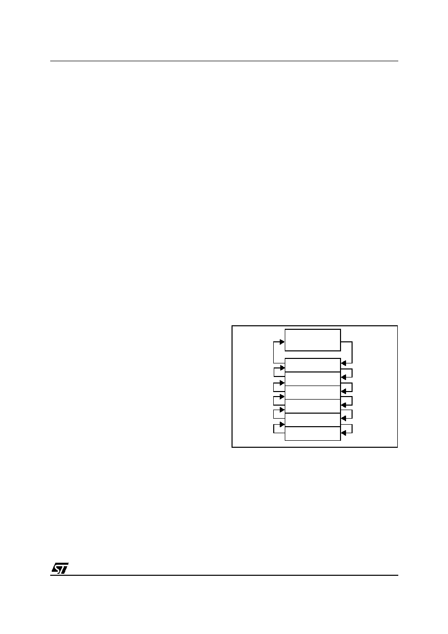
Figure 1. Block Diagram
NMI
INTERRUPTS
PROGRAM
PC
STACK LEVEL 1
STACK LEVEL 2
STACK LEVEL 3
STACK LEVEL 4
STACK LEVEL 5
STACK LEVEL 6
POWER
SUPPLY
OSCILLATOR
RESET
DATA ROM
USER
SELECTABLE
DATA RAM
64 Bytes
PORT A
PORT B
TIMER
8-BIT CORE
8-BIT *
A/D CONVERTER
PA1..PA3 (20mA Sink)
PB0..PB1
V
DD
V
SS
OSCin OSCout
RESET
WATCHDOG
:
MEMORY
TIMER
(1K or 2K Bytes)
PB3, PB5..PB7 / Ain*
* Depending on device. Please refer to I/O Port section.
V
PP
4
ST6200C/ST6201C/ST6203C
7/100
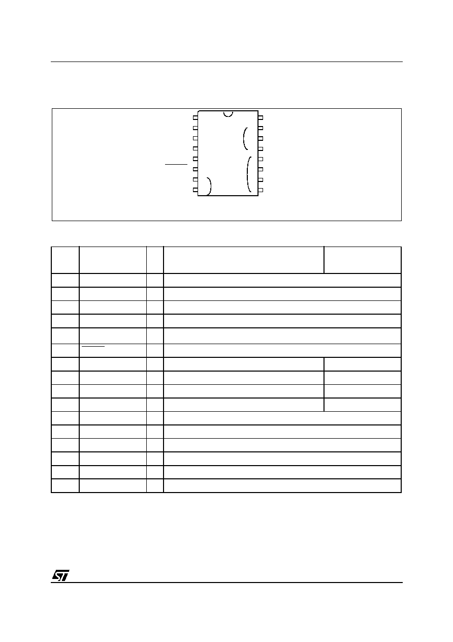
2 PIN DESCRIPTION
Figure 2. 16-Pin Package Pinout
Table 1. Device Pin Description
Legend / Abbreviations for
Table 1
:
* Depending on device. Please refer to I/O Port section.
I = input, O = output, S = supply, IPU = input pull-up
The input with pull-up configuration (reset state) is valid as long as the user software does not change it.
Refer to
Section 7 "I/O PORTS" on page 36
for more details on the software configuration of the I/O ports.
16
15
14
13
12
11
10
9
1
2
3
4
5
6
7
8
V
DD
PB5/Ain*
Ain*/PB6
Ain*/PB7
RESET
V
PP
NMI
OSCout
OSCin
V
SS
PB3/Ain*
PB1
PB0
PA3/20mA Sink
PA2/20mA Sink
PA1/20mA Sink
it2
it1
itX associated interrupt vector
* Depending on device. Please refer to I/O Port section.
it2
Pin n∞
Pin Name
Typ
e
Main Function
(after Reset)
Alternate Function
1 V
DD
S
Main power supply
2
OSCin
I
External clock input or resonator oscillator inverter input
3
OSCout
O
Resonator oscillator inverter output or resistor input for RC oscillator
4
NMI
I
Non maskable interrupt (falling edge sensitive)
5
V
PP
Must be held at Vss for normal operation, if a 12.5V level is applied to the pin
during the reset phase, the device enters EPROM programming mode.
6
RESET
I/O Top priority non maskable interrupt (active low)
7
PB7/Ain*
I/O Pin B7 (IPU)
Analog input
8
PB6/Ain*
I/O Pin B6 (IPU)
Analog input
9
PB5/Ain*
I/O Pin B5 (IPU)
Analog input
10
PB3/Ain*
I/O Pin B3 (IPU)
Analog input
11
PB1
I/O Pin B1 (IPU)
12
PB0
I/O Pin B0 (IPU)
13
PA3/ 20mA Sink
I/O Pin A3 (IPU)
14
PA2/ 20mA Sink
I/O Pin A2 (IPU)
15
PA1/ 20mA Sink
I/O Pin A1 (IPU)
16
V
SS
S Ground
ST6200C/ST6201C/ST6203C
8/100
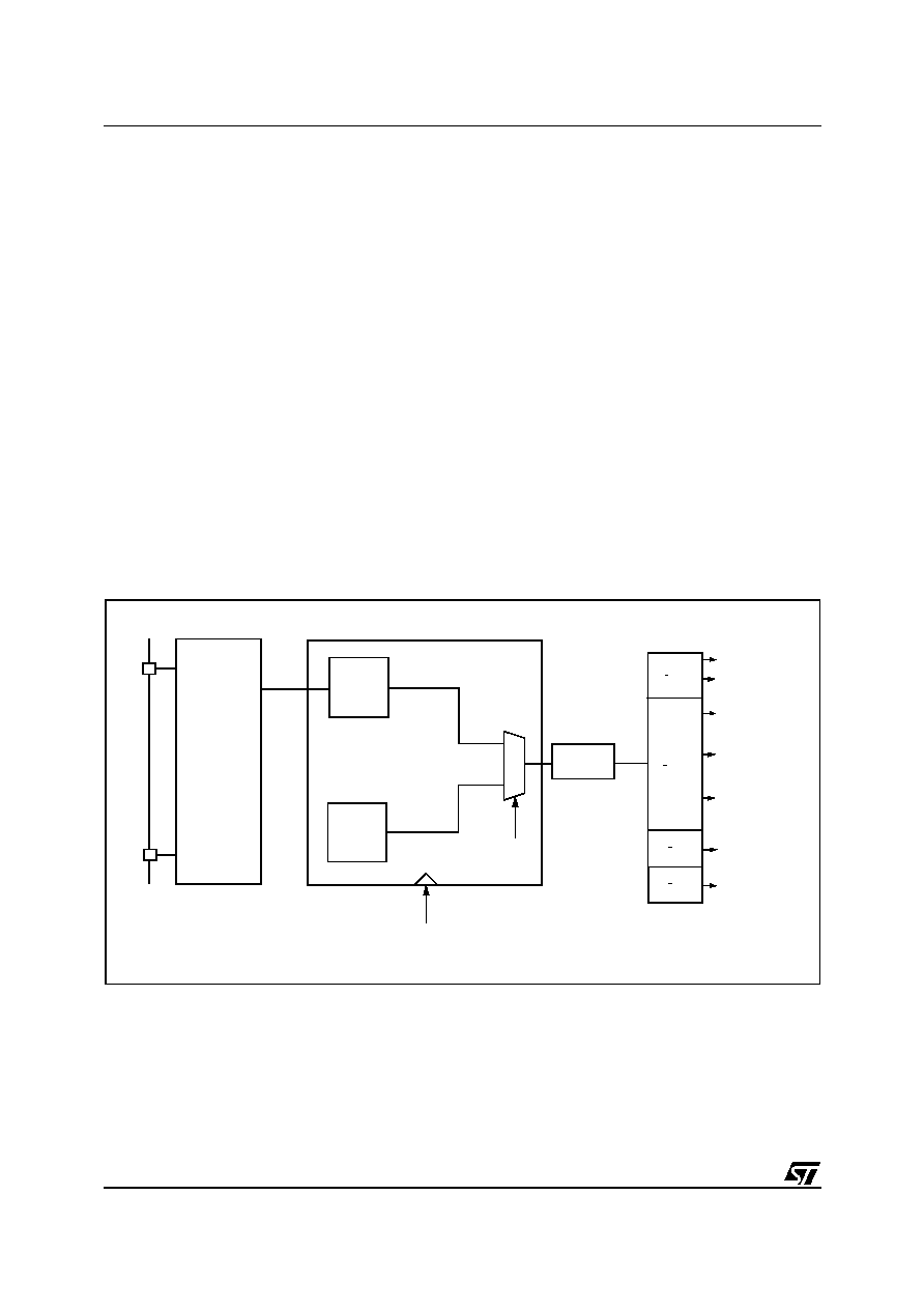
3 MEMORY MAPS, PROGRAMMING MODES AND OPTION BYTES
3.1 MEMORY AND REGISTER MAPS
3.1.1 Introduction
The MCU operates in three separate memory
spaces: Program space, Data space, and Stack
space. Operation in these three memory spaces is
described in the following paragraphs.
Briefly, Program space contains user program
code in OTP and user vectors; Data space con-
tains user data in RAM and in OTP, and Stack
space accommodates six levels of stack for sub-
routine and interrupt service routine nesting.
Figure 3. Memory Addressing Diagram
PROGRAM SPACE
PROGRAM
INTERRUPT &
RESET VECTORS
ACCUMULATOR
RAM
X REGISTER
Y REGISTER
V REGISTER
W REGISTER
000h
03Fh
040h
07Fh
080h
081h
082h
083h
084h
0C0h
0FFh
DATA SPACE
000h
0FF0h
0FFFh
MEMORY
WINDOW
DATA ROM
RESERVED
HARDWARE
CONTROL
REGISTERS
0BFh
(see
Table 2
)
(see
Figure 4
)
1
ST6200C/ST6201C/ST6203C
9/100
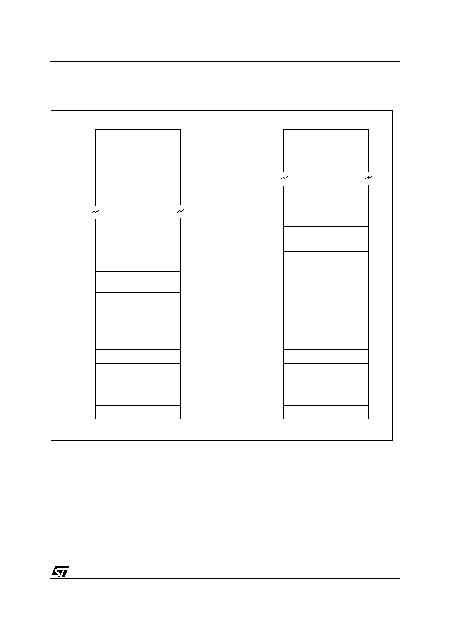
MEMORY MAP (Cont'd)
Figure 4. Program Memory Map
(*) Reserved areas should be filled with 0FFh
0000h
0AFFh
0B00h
0B9Fh
RESERVED
*
USER
PROGRAM MEMORY
1024 BYTES
0BA0h
0F9Fh
0FA0h
0FEFh
0FF0h
0FF7h
0FF8h
0FFBh
0FFCh
0FFDh
0FFEh
0FFFh
RESERVED
*
RESERVED*
INTERRUPT VECTORS
NMI VECTOR
USER RESET VECTOR
0000h
07FFh
0800h
087Fh
RESERVED
*
USER
PROGRAM MEMORY
1824 BYTES
0880h
0F9Fh
0FA0h
0FEFh
0FF0h
0FF7h
0FF8h
0FFBh
0FFCh
0FFDh
0FFEh
0FFFh
RESERVED
*
RESERVED*
INTERRUPT VECTORS
NMI VECTOR
USER RESET VECTOR
ST62T03C,T00C
ST62T01C, E01C
NOT IMPLEMENTED
NOT IMPLEMENTED
1

ST6200C/ST6201C/ST6203C
10/100
MEMORY MAP (Cont'd)
3.1.2 Program Space
Program Space comprises the instructions to be
executed, the data required for immediate ad-
dressing mode instructions, the reserved factory
test area and the user vectors. Program Space is
addressed via the 12-bit Program Counter register
(PC register). Thus, the MCU is capable of ad-
dressing 4K bytes of memory directly.
3.1.3 Readout Protection
The Program Memory in in OTP, EPROM or ROM
devices can be protected against external readout
of memory by setting the Readout Protection bit in
the option byte (
Section 3.3 on page 15
).
In the EPROM parts, Readout Protection option
can be desactivated only by U.V. erasure that also
results in the whole EPROM context being erased.
Note: Once the Readout Protection is activated, it
is no longer possible, even for STMicroelectronics,
to gain access to the OTP or ROM contents. Re-
turned parts can therefore not be accepted if the
Readout Protection bit is set.
3.1.4 Data Space
Data Space accommodates all the data necessary
for processing the user program. This space com-
prises the RAM resource, the processor core and
peripheral registers, as well as read-only data
such as constants and look-up tables in OTP/
EPROM.
3.1.4.1 Data ROM
All read-only data is physically stored in program
memory, which also accommodates the Program
Space. The program memory consequently con-
tains the program code to be executed, as well as
the constants and look-up tables required by the
application.
The Data Space locations in which the different
constants and look-up tables are addressed by the
processor core may be thought of as a 64-byte
window through which it is possible to access the
read-only data stored in OTP/EPROM.
3.1.4.2 Data RAM
The data space includes the user RAM area, the
accumulator (A), the indirect registers (X), (Y), the
short direct registers (V), (W), the I/O port regis-
ters, the peripheral data and control registers, the
interrupt option register and the Data ROM Win-
dow register (DRWR register).
3.1.5 Stack Space
Stack space consists of six 12-bit registers which
are used to stack subroutine and interrupt return
addresses, as well as the current program counter
contents.
1
ST6200C/ST6201C/ST6203C
11/100
MEMORY MAP (Cont'd)
Table 2. Hardware Register Map
Legend:
x = undefined, R/W = Read/Write, Ro = Read-only Bit(s) in the register, Wo = Write-only Bit(s)
in the register.
Notes:
1. The contents of the I/O port DR registers are readable only in output configuration. In input configura-
tion, the values of the I/O pins are returned instead of the DR register contents.
2. The bits associated with unavailable pins must always be kept at their reset value.
3. Do not use single-bit instructions (SET, RES...) on Port Data Registers if any pin of the port is configured
in input mode (refer to
Section 7 "I/O PORTS" on page 36
for more details).
4. Depending on device. See device summary on page 1.
Address
Block
Register
Label
Register Name
Reset
Status
Remarks
080h
to 083h
CPU
X,Y,V,W
X,Y index registers
V,W short direct registers
xxh
R/W
0C0h
0C1h
I/O Ports
DRA
1) 2) 3)
DRB
1) 2) 3)
Port A Data Register
Port B Data Register
00h
00h
R/W
R/W
0C2h
0C3h
Reserved (2 Bytes)
0C4h
0C5h
I/O Ports
DDRA
2)
DDRB
2)
Port A Direction Register
Port B Direction Register
00h
00h
R/W
R/W
0C6h
0C7h
Reserved (2 Bytes)
0C8h
CPU
IOR
Interrupt Option Register
xxh
Write-only
0C9h
ROM
DRWR
Data ROM Window register
xxh
Write-only
0CAh
0CBh
Reserved (2 Bytes)
0CCh
0CDh
I/O Ports
ORA
2)
ORB
2)
Port A Option Register
Port B Option Register
00h
00h
R/W
R/W
0CEh
0CFh
Reserved (2 bytes)
0D0h
0D1h
ADC
ADR
ADCR
A/D Converter Data Register
A/D Converter Control Register
xxh
40h
Read-only
Ro/Wo
0D2h
0D3h
0D4h
Timer 1
PSCR
TCR
TSCR
Timer 1 Prescaler Register
Timer 1 Downcounter Register
Timer 1 Status Control Register
7Fh
0FFh
00h
R/W
R/W
R/W
0D5h
to 0D7h
Reserved (3 Bytes)
0D8h
Watchdog
Timer
WDGR
Watchdog Register
0FEh
R/W
0D9h
to 0FEh
Reserved (38 Bytes)
0FFh
CPU
A
Accumulator
xxh
R/W
1
ST6200C/ST6201C/ST6203C
12/100
MEMORY MAP (Cont'd)
3.1.6 Data ROM Window
The Data read-only memory window is located
from address 0040h to address 007Fh in Data
space. It allows direct reading of 64 consecutive
bytes located anywhere in program memory, be-
tween address 0000h and 0FFFh.
There are 64 blocks of 64 bytes in a 4K device:
≠ Block 0 is related to the address range 0000h to
003Fh.
≠ Block 1 is related to the address range 0040h to
007Fh.
and so on...
All the program memory can therefore be used to
store either instructions or read-only data. The
Data ROM window can be moved in steps of 64
bytes along the program memory by writing the
appropriate code in the Data ROM Window Regis-
ter (DRWR).
Figure 5. Data ROM Window
3.1.6.1 Data ROM Window Register (DRWR)
The DRWR can be addressed like any RAM loca-
tion in the Data Space.
This register is used to select the 64-byte block of
program memory to be read in the Data ROM win-
dow (from address 40h to address 7Fh in Data
space). The DRWR register is not cleared on re-
set, therefore it must be written to before access-
ing the Data read-only memory window area for
the first time.
Address: 0C9h
--
Write Only
Reset Value = xxh (undefined)
Bits 7:6 = Reserved, must be cleared.
Bit 5:0 = DRWR[5:0]
Data read-only memory Win-
dow Register Bits.
These are the Data read-only
memory Window bits that correspond to the upper
bits of the data read-only memory space.
Caution:
This register is undefined on reset, it is
write-only, therefore do not read it nor access it us-
ing Read-Modify-Write instructions (SET, RES,
INC and DEC).
0000h
0FFFh
000h
040h
07Fh
0FFh
DATA ROM
WINDOW
DATA SPACE
64-BYTE
ROM
PROGRAM
SPACE
7
0
-
-
DRWR5 DRWR4 DRWR3 DRWR2 DRWR1 DRWR0
1
ST6200C/ST6201C/ST6203C
13/100
MEMORY MAP (Cont'd)
3.1.6.2 Data ROM Window memory addressing
In cases where some data (look-up tables for ex-
ample) are stored in program memory, reading
these data requires the use of the Data ROM win-
dow mechanism. To do this:
1. The DRWR register has to be loaded with the
64-byte block number where the data are located
(in program memory). This number also gives the
start address of the block.
2. Then, the offset address of the byte in the Data
ROM Window (corresponding to the offset in the
64-byte block in program memory) has to be load-
ed in a register (A, X,...).
When the above two steps are completed, the
data can be read.
To understand how to determine the DRWR and
the content of the register, please refer to the ex-
ample shown in
Figure 6
. In any case the calcula-
tion is automatically handled by the ST6 develop-
ment tools.
Please refer to the user manual of the correspod-
ing tool.
3.1.6.3 Recommendations
Care is required when handling the DRWR regis-
ter as it is write only. For this reason, the DRWR
contents should not be changed while executing
an interrupt service routine, as the service routine
cannot save and then restore the register's previ-
ous contents. If it is impossible to avoid writing to
the DRWR during the interrupt service routine, an
image of the register must be saved in a RAM lo-
cation, and each time the program writes to the
DRWR, it must also write to the image register.
The image register must be written first so that, if
an interrupt occurs between the two instructions,
the DRWR is not affected.
Figure 6. Data ROM Window Memory Addressing
DATA
PROGRAM SPACE
DATA SPACE
0000h
0400h
0421h
07FFh
64 bytes
OFFSET
000h
040h
061h
07Fh
OFFSET
21h
0FFh
DRWR
DATA address in Program memory : 421h
DRWR content : 421h / 3Fh (64) = 10H data is located in 64-bytes window number 10h
64-byte window start address : 10h x 3Fh = 400h
Register (A, X,...)content : Offset = (421h - 400h) + 40h ( Data ROM Window start address in data space) = 61h
10h
DATA
1

ST6200C/ST6201C/ST6203C
14/100
3.2 PROGRAMMING MODES
3.2.1 Program Memory
EPROM/OTP programming mode is set by a
+12.5V voltage applied to the TEST/V
PP
pin. The
programming flow of the ST62T00C, T01/E01C
and T03C is described in the User Manual of the
EPROM Programming Board.
Table 3. ST6200C/03C Program Memory Map
Table 4. ST6201C Program Memory Map
Note: OTP/EPROM devices can be programmed
with the development tools available from
STMicroelectronics (please refer to
Section 12 on
page 95
).
3.2.2 EPROM Erasing
The EPROM devices can be erased by exposure
to Ultra Violet light. The characteristics of the MCU
are such that erasure begins when the memory is
exposed to light with a wave lengths shorter than
approximately 4000≈. It should be noted that sun-
light and some types of fluorescent lamps have
wavelengths in the range 3000-4000≈.
It is thus recommended that the window of the
MCU packages be covered by an opaque label to
prevent unintentional erasure problems when test-
ing the application in such an environment.
The recommended erasure procedure is exposure
to short wave ultraviolet light which have a wave-
length 2537≈. The integrated dose (i.e. U.V. inten-
sity x exposure time) for erasure should be a mini-
mum of 30W-sec/cm
2
. The erasure time with this
dosage is approximately 30 to 40 minutes using an
ultraviolet lamp with 12000µW/cm
2
power rating.
The EPROM device should be placed within
2.5cm (1inch) of the lamp tubes during erasure.
Device Address
Description
0000h-0B9Fh
0BA0h-0F9Fh
0FA0h-0FEFh
0FF0h-0FF7h
0FF8h-0FFBh
0FFCh-0FFDh
0FFEh-0FFFh
Reserved
User ROM
Reserved
Interrupt Vectors
Reserved
NMI Interrupt Vector
Reset Vector
Device Address
Description
0000h-087Fh
0880h-0F9Fh
0FA0h-0FEFh
0FF0h-0FF7h
0FF8h-0FFBh
0FFCh-0FFDh
0FFEh-0FFFh
Reserved
User ROM
Reserved
Interrupt Vectors
Reserved
NMI Interrupt Vector
Reset Vector
1

ST6200C/ST6201C/ST6203C
15/100
3.3 OPTION BYTES
Each device is available for production in user pro-
grammable versions (OTP) as well as in factory
coded versions (ROM). OTP devices are shipped
to customers with a default content (00h), while
ROM factory coded parts contain the code sup-
plied by the customer. This implies that OTP de-
vices have to be configured by the customer using
the Option Bytes while the ROM devices are facto-
ry-configured.
The two option bytes allow the hardware configu-
ration of the microcontroller to be selected.
The option bytes have no address in the memory
map and can be accessed only in programming
mode (for example using a standard ST6 program-
ming tool).
In masked ROM devices, the option bytes are
fixed in hardware by the ROM code (see
Section
11.6.2 "ROM VERSION" on page 93
). It is there-
fore impossible to read the option bytes.
The option bytes can be only programmed once. It
is not possible to change the selected options after
they have been programmed.
In order to reach the power consumption value in-
dicated in
Section 10.4
, the option byte must be
programmed to its default value. Otherwise, an
over-consumption will occur.
MSB OPTION BYTE
Bits 15:11 = Reserved, must be always cleared.
Bit 10 = Reserved, must be always set.
Bit 9 = EXTCNTL
External STOP MODE control.
0: EXTCNTL mode not available. STOP mode is
not available with the watchdog active.
1: EXTCNTL mode available. STOP mode is avail-
able with the watchdog active by setting NMI pin
to one.
Bit 8 = LVD
Low Voltage Detector
on/off
.
This option bit enable or disable the Low Voltage
Detector (LVD) feature.
0: Low Voltage Detector disabled
1: Low Voltage Detector enabled.
LSB OPTION BYTE
Bit 7 = PROTECT
Readout Protection.
This option bit enables or disables external access
to the internal program memory.
0: Program memory not read-out protected
1: Program memory read-out protected
Bit 6 = OSC
Oscillator selection
.
This option bit selects the main oscillator type.
0: Quartz crystal, ceramic resonator or external
clock
1: RC network
Bit 5 = Reserved, must be always cleared.
Bit 4 = Reserved, must be always set.
Bit 3 = NMI PULL
NMI Pull-Up
on/off.
This option bit enables or disables the internal pull-
up on the NMI pin.
0: Pull-up disabled
1: Pull-up enabled
Bit 2 = Reserved, must be always set.
Bit 1 = WDACT
Hardware or software watchdog.
This option bit selects the watchdog type.
0: Software (watchdog to be enabled by software)
1: Hardware (watchdog always enabled)
Bit 0 = OSGEN
Oscillator Safeguard
on/off.
This option bit enables or disables the oscillator
Safeguard (OSG) feature.
0: Oscillator Safeguard disabled
1: Oscillator Safeguard enabled
MSB OPTION BYTE
15
8
LSB OPTION BYTE
7
0
Reserved
EXT
CTL
LVD
PRO-
TECT
OSC Res.
Res.
NMI
PULL
Res.
WD
ACT
OSG
EN
Default
Value
X
X
X
X
X
X
X
X
X
X
X
X
X
X
X
X
1
ST6200C/ST6201C/ST6203C
16/100
4 CENTRAL PROCESSING UNIT
4.1 INTRODUCTION
The CPU Core of ST6 devices is independent of the
I/O or Memory configuration. As such, it may be
thought of as an independent central processor
communicating with on-chip I/O, Memory and Pe-
ripherals via internal address, data, and control
buses.
4.2 MAIN FEATURES
s
40 basic instructions
s
9 main addressing modes
s
Two 8-bit index registers
s
Two 8-bit short direct registers
s
Low power modes
s
Maskable hardware interrupts
s
6-level hardware stack
4.3 CPU REGISTERS
The ST6 Family CPU core features six registers and
three pairs of flags available to the programmer.
These are described in the following paragraphs.
Accumulator (A). The accumulator is an 8-bit
general purpose register used in all arithmetic cal-
culations, logical operations, and data manipula-
tions. The accumulator can be addressed in Data
Space as a RAM location at address FFh. Thus
the ST6 can manipulate the accumulator just like
any other register in Data Space.
Index Registers (X, Y). These two registers are
used in Indirect addressing mode as pointers to
memory locations in Data Space. They can also
be accessed in Direct, Short Direct, or Bit Direct
addressing modes. They are mapped in Data
Space at addresses 80h (X) and 81h (Y) and can
be accessed like any other memory location.
Short Direct Registers (V, W). These two regis-
ters are used in Short Direct addressing mode.
This means that the data stored in V or W can be
accessed with a one-byte instruction (four CPU cy-
cles). V and W can also be accessed using Direct
and Bit Direct addressing modes. They are
mapped in Data Space at addresses 82h (V) and
83h (W) and can be accessed like any other mem-
ory location.
Note: The X and Y registers can also be used as
Short Direct registers in the same way as V and W.
Program Counter (PC). The program counter is a
12-bit register which contains the address of the
next instruction to be executed by the core. This
ROM location may be an opcode, an operand, or
the address of an operand.
Figure 7. CPU Registers
ACCUMULATOR
X INDEX REGISTER
Y INDEX REGISTER
PROGRAM COUNTER
RESET VALUE = RESET VECTOR @ 0FFEh-0FFFh
7
0
7
0
7
0
0
11
RESET VALUE = xxh
RESET VALUE = xxh
RESET VALUE = xxh
x = Undefined value
V SHORT INDIRECT
7
0
RESET VALUE = xxh
W SHORT INDIRECT
7
0
RESET VALUE = xxh
NORMAL FLAGS
CN
ZN
CI
ZI
CNMI ZNMI
INTERRUPT FLAGS
NMI FLAGS
SIX LEVEL
STACK
REGISTER
REGISTER
1
ST6200C/ST6201C/ST6203C
17/100
CPU REGISTERS (Cont'd)
The 12-bit length allows the direct addressing of
4096 bytes in Program Space.
However, if the program space contains more than
4096 bytes, the additional memory in program
space can be addressed by using the Program
ROM Page register.
The PC value is incremented after reading the ad-
dress of the current instruction. To execute relative
jumps, the PC and the offset are shifted through
the ALU, where they are added; the result is then
shifted back into the PC. The program counter can
be changed in the following ways:
≠ JP (Jump) instruction
PC = Jump address
≠ CALL instruction
PC = Call address
≠ Relative Branch InstructionPC = PC +/- offset
≠ Interrupt
PC = Interrupt vector
≠ Reset
PC = Reset vector
≠ RET & RETI instructions
PC = Pop (stack)
≠ Normal instruction
PC = PC + 1
Flags (C, Z). The ST6 CPU includes three pairs of
flags (Carry and Zero), each pair being associated
with one of the three normal modes of operation:
Normal mode, Interrupt mode and Non Maskable
Interrupt mode. Each pair consists of a CARRY
flag and a ZERO flag. One pair (CN, ZN) is used
during Normal operation, another pair is used dur-
ing Interrupt mode (CI, ZI), and a third pair is used
in the Non Maskable Interrupt mode (CNMI, ZN-
MI).
The ST6 CPU uses the pair of flags associated
with the current mode: as soon as an interrupt (or
a Non Maskable Interrupt) is generated, the ST6
CPU uses the Interrupt flags (or the NMI flags) in-
stead of the Normal flags. When the RETI instruc-
tion is executed, the previously used set of flags is
restored. It should be noted that each flag set can
only be addressed in its own context (Non Maska-
ble Interrupt, Normal Interrupt or Main routine).
The flags are not cleared during context switching
and thus retain their status.
C : Carry flag.
This bit is set when a carry or a borrow occurs dur-
ing arithmetic operations; otherwise it is cleared.
The Carry flag is also set to the value of the bit
tested in a bit test instruction; it also participates in
the rotate left instruction.
0: No carry has occured
1: A carry has occured
Z : Zero flag
This flag is set if the result of the last arithmetic or
logical operation was equal to zero; otherwise it is
cleared.
0: The result of the last operation is different from
zero
1: The result of the last operation is zero
Switching between the three sets of flags is per-
formed automatically when an NMI, an interrupt or
a RETI instruction occurs. As NMI mode is auto-
matically selected after the reset of the MCU, the
ST6 core uses the NMI flags first.
Stack. The ST6 CPU includes a true LIFO (Last In
First Out) hardware stack which eliminates the
need for a stack pointer. The stack consists of six
separate 12-bit RAM locations that do not belong
to the data space RAM area. When a subroutine
call (or interrupt request) occurs, the contents of
each level are shifted into the next level down,
while the content of the PC is shifted into the first
level (the original contents of the sixth stack level
are lost). When a subroutine or interrupt return oc-
curs (RET or RETI instructions), the first level reg-
ister is shifted back into the PC and the value of
each level is popped back into the previous level.
Figure 8. Stack manipulation
Since the accumulator, in common with all other
data space registers, is not stored in this stack,
management of these registers should be per-
formed within the subroutine.
Caution: The stack will remain in its "deepest" po-
sition if more than 6 nested calls or interrupts are
executed, and consequently the last return ad-
dress will be lost.
It will also remain in its highest position if the stack
is empty and a RET or RETI is executed. In this
case the next instruction will be executed.
LEVEL 1
LEVEL 2
LEVEL 3
LEVEL 4
LEVEL 5
LEVEL 6
ON
INTERRUPT,
OR
SUBROUTINE
CALL
ON RETURN
FROM
INTERRUPT,
OR
SUBROUTINE
PROGRAM
COUNTER
1
ST6200C/ST6201C/ST6203C
18/100
5 CLOCKS, SUPPLY AND RESET
5.1 CLOCK SYSTEM
The main oscillator of the MCU can be driven by
any of these clock sources:
≠ external clock signal
≠ external AT-cut parallel-resonant crystal
≠ external ceramic resonator
≠ external RC network (R
NET
).
In addition, an on-chip Low Frequency Auxiliary
Oscillator (LFAO) is available as a back-up clock
system or to reduce power consumption.
An optional Oscillator Safeguard (OSG) filters
spikes from the oscillator lines, and switches to the
LFAO backup oscillator in the event of main oscil-
lator failure. It also automatically limits the internal
clock frequency (f
INT
) as a function of V
DD
, in order
to guarantee correct operation. These functions
are illustrated in
Figure 10
, and
Figure 11
.
Table 5
illustrates various possible oscillator con-
figurations using an external crystal or ceramic
resonator, an external clock input, an external re-
sistor (R
NET
), or the lowest cost solution using only
the LFAO.
For more details on configuring the clock options,
refer to the Option Bytes section of this document.
The internal MCU clock frequency (f
INT
) is divided
by 12 to drive the Timer, the Watchdog timer and
the A/D converter, by 13 to drive the CPU core and
the SPI and by 1 or 3 to drive the ARTIMER, as
shown in
Figure 9
.
With an 8 MHz oscillator, the fastest CPU cycle is
therefore 1.625µs.
A CPU cycle is the smallest unit of time needed to
execute any operation (for instance, to increment
the Program Counter). An instruction may require
two, four, or five CPU cycles for execution.
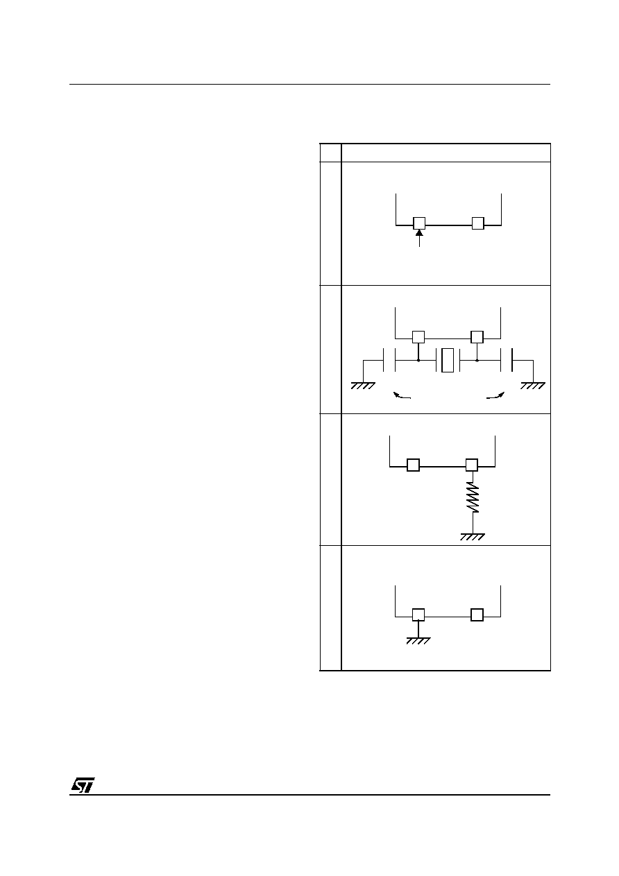
Figure 9. Clock Circuit Block Diagram
MAIN
OSCILLATOR
OSG
LFAO
CORE
: 13
: 12
8-BIT TIMER
WATCHDOG
f
INT
OSCOFF BIT
ADC
0
1
filtering
OSCILLATOR SAFEGUARD (OSG)
OSG ENABLE OPTION BIT (See OPTION BYTE SECTION)
(ADCR REGISTER)
f
OSC
* Depending on device. See device summary on page 1.
*
*
Oscillator
Divider
SPI
: 1
: 3
8-BIT ARTIMER
8-BIT ARTIMER
1
ST6200C/ST6201C/ST6203C
19/100
CLOCK SYSTEM (Cont'd)
5.1.1 Main Oscillator
The oscillator configuration is specified by select-
ing the appropriate option in the option bytes (refer
to the Option Bytes section of this document).
When the CRYSTAL/RESONATOR option is se-
lected, it must be used with a quartz crystal, a ce-
ramic resonator or an external signal provided on
the OSCin pin. When the RC NETWORK option is
selected, the system clock is generated by an ex-
ternal resistor (the capacitor is implemented inter-
nally).
The main oscillator can be turned off (when the
OSG ENABLED option is selected) by setting the
OSCOFF bit of the ADC Control Register (not
available on some devices). This will automatically
start the Low Frequency Auxiliary Oscillator
(LFAO).
The main oscillator can be turned off by resetting
the OSCOFF bit of the A/D Converter Control Reg-
ister or by resetting the MCU. When the main os-
cillator starts there is a delay made up of the oscil-
lator start-up delay period plus the duration of the
software instruction at a clock frequency f
LFAO
.
Caution: It should be noted that when the RC net-
work option is selected, the accuracy of the fre-
quency is about 20% so it may not be suitable for
some applications (For more details, please refer
to the Electrical Characteristics Section).
Table 5. Oscillator Configurations
Notes:
1. To select the options shown in column 1 of the above
table, refer to the Option Byte section.
2.This schematic are given for guidance only and are sub-
ject to the schematics given by the crystal or ceramic res-
onator manufacturer.
3. For more details, please refer to the Electrical Charac-
teristics Section.
Hardware Configuration
Crys
tal/Re
sona
tor O
ption
1)
Cr
ystal/
Reso
nator
Optio
n
1)
RC
Netwo
rk O
ption
1)
O
SG E
nable
d Op
tion
1)
OSCin
OSCout
EXTERNAL
ST6
CLOCK
NC
External Clock
OSCin
OSCout
LOAD
CAPACITORS
3)
ST6
C
L2
C
L1
Crystal/Resonator Clock
2)
OSCin
OSCout
ST6
R
NET
NC
RC Network
OSCin
OSCout
ST6
LFAO
NC
1
ST6200C/ST6201C/ST6203C
20/100
CLOCK SYSTEM (Cont'd)
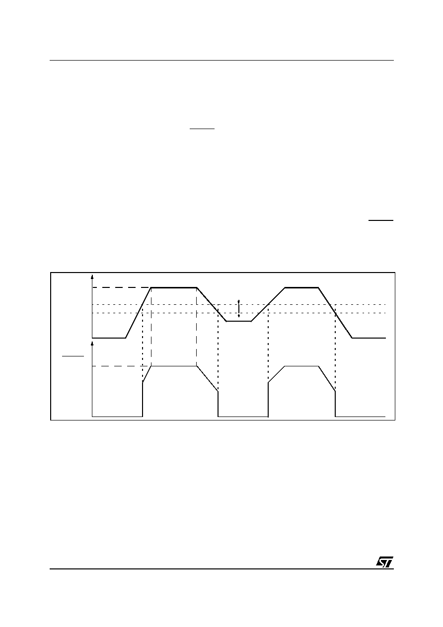
5.1.2 Oscillator Safeguard (OSG)
The Oscillator Safeguard (OSG) feature is a
means of dramatically improving the operational
integrity of the MCU. It is available when the OSG
ENABLED option is selected in the option byte (re-
fer to the Option Bytes section of this document).
The OSG acts as a filter whose cross-over fre-
quency is device dependent and provides three
basic functions:
≠ Filtering spikes on the oscillator lines which
would result in driving the CPU at excessive fre-
quencies
≠ Management of the Low Frequency Auxiliary
Oscillator (LFAO), (useable as low cost internal
clock source, backup clock in case of main oscil-
lator failure or for low power consumption)
≠ Automatically limiting the f
INT
clock frequency as
a function of supply voltage, to ensure correct
operation even if the power supply drops.
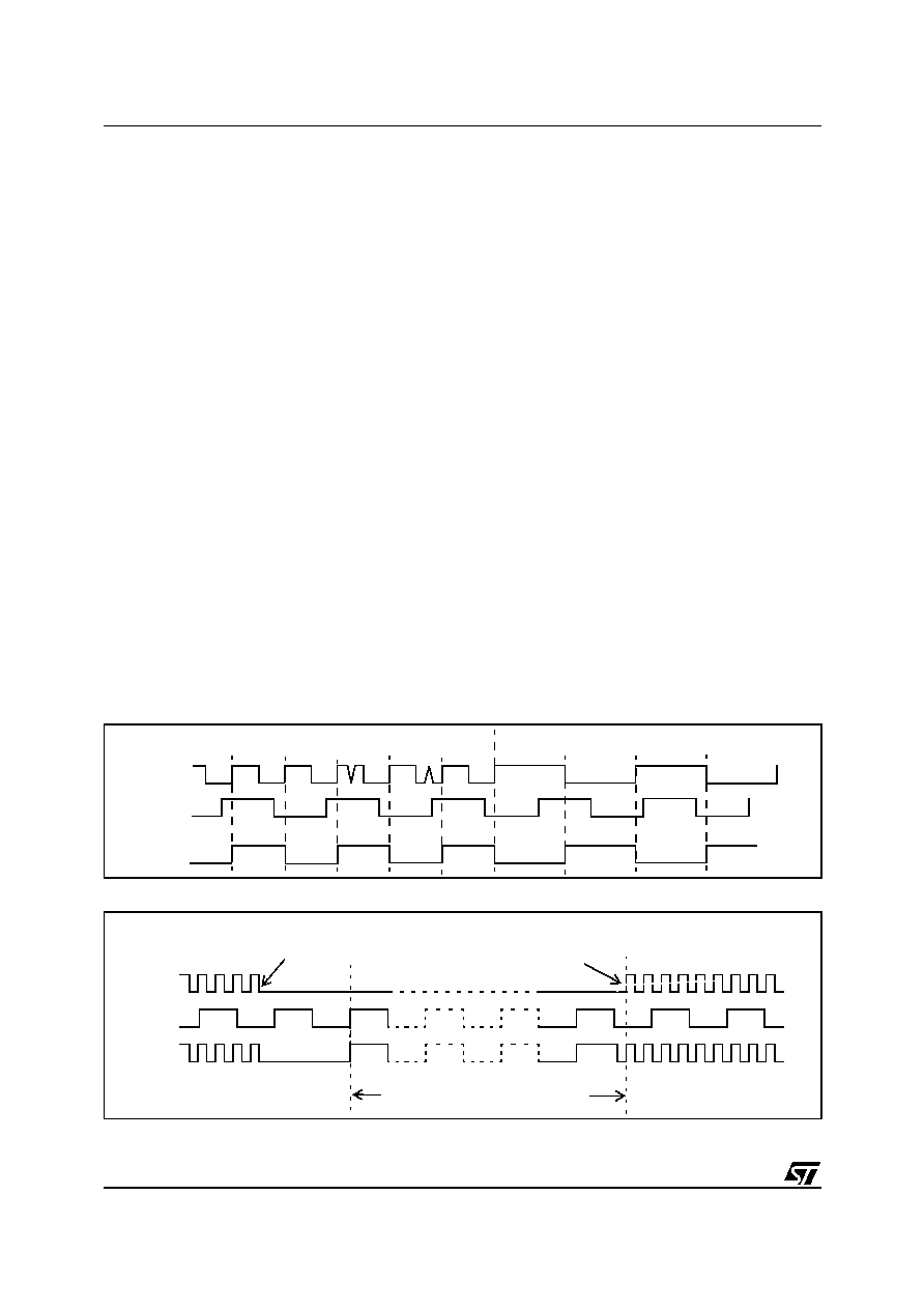
5.1.2.1 Spike Filtering
Spikes on the oscillator lines result in an effectively
increased internal clock frequency. In the absence
of an OSG circuit, this may lead to an over fre-
quency for a given power supply voltage. The
OSG filters out such spikes (as illustrated in
Figure
10
). In all cases, when the OSG is active, the max-
imum internal clock frequency, f
INT
, is limited to
f
OSG
, which is supply voltage dependent.
5.1.2.2 Management of Supply Voltage
Variations
Over-frequency, at a given power supply level, is
seen by the OSG as spikes; it therefore filters out
some cycles in order that the internal clock fre-
quency of the device is kept within the range the
particular device can stand (depending on V
DD
),
and below f
OSG
: the maximum authorised frequen-
cy with OSG enabled.
5.1.2.3 LFAO Management
When the OSG is enabled, the Low Frequency
Auxiliary Oscillator can be used (see
Section
5.1.3
).
Note:
The OSG should be used wherever possible
as it provides maximum security for the applica-
tion. It should be noted however, that it can in-
crease power consumption and reduce the maxi-
mum operating frequency to f
OSG
(see Electrical
Characteristics section).
Caution: Care has to be taken when using the
OSG, as the internal frequency is defined between
a minimum and a maximum value and may vary
depending on both V
DD
and temperature. For pre-
cise timing measurements, it is not recommended
to use the OSG.
Figure 10. OSG Filtering Function
Figure 11. LFAO Oscillator Function
f
OSC
f
OSG
f
INT
f
OSC<
f
OSG
f
OSC>
f
OSG
MAIN OSCILLATOR
STOPS
MAIN OSCILLATOR
RESTARTS
INTERNAL CLOCK DRIVEN BY LFAO
f
OSC
f
INT
f
LFAO
1

ST6200C/ST6201C/ST6203C
21/100
CLOCK SYSTEM (Cont'd)
5.1.3 Low Frequency Auxiliary Oscillator
(LFAO)
The Low Frequency Auxiliary Oscillator has three
main purposes. Firstly, it can be used to reduce
power consumption in non timing critical routines.
Secondly, it offers a fully integrated system clock,
without any external components. Lastly, it acts as
a backup oscillator in case of main oscillator fail-
ure.
This oscillator is available when the OSG ENA-
BLED option is selected in the option byte (refer to
the Option Bytes section of this document). In this
case, it automatically starts one of its periods after
the first missing edge of the main oscillator, what-
ever the reason for the failure (main oscillator de-
fective, no clock circuitry provided, main oscillator
switched off...). See
Figure 11
.
User code, normal interrupts, WAIT and STOP in-
structions, are processed as normal, at the re-
duced f
LFAO
frequency. The A/D converter accura-
cy is decreased, since the internal frequency is be-
low 1.2 MHz.
At power on, until the main oscillator starts, the re-
set delay counter is driven by the LFAO. If the
main oscillator starts before the 2048 or 32768 cy-
cle delay has elapsed, it takes over.
The Low Frequency Auxiliary Oscillator is auto-
matically switched off as soon as the main oscilla-
tor starts.
5.1.4 Register Description
ADC CONTROL REGISTER (ADCR)
Address: 0D1h
--
Read/Write
Reset value: 0100 0000 (40h)
Bit 7:3, 1:0 = ADCR[7:3], ADCR[1:0]
ADC Control
Register
.
These bits are used to control the A/D converter (if
available on the device) otherwise they are not
used.
Bit 2 = OSCOFF
Main Oscillator Off.
0: Main oscillator enabled
1: Main oscillator disabled
Note: The OSG must be enabled using the OS-
GEN option in the Option Byte, otherwise the OS-
COFF setting has no effect.
7
0
ADCR
7
ADCR
6
ADCR
5
ADCR
4
ADCR
3
OSC
OFF
ADCR
1
ADCR
0
1
ST6200C/ST6201C/ST6203C
22/100
5.2 LOW VOLTAGE DETECTOR (LVD)
The on-chip Low Voltage Detector is enabled by
setting a bit in the option bytes (refer to the Option
Bytes section of this document).
The LVD allows the device to be used without any
external RESET circuitry. In this case, the RESET
pin should be left unconnected.
If the LVD is not used, an external circuit is manda-
tory to ensure correct Power On Reset operation,
see figure in the Reset section. For more details,
please refer to the application note AN669.
The LVD generates a static Reset when the supply
voltage is below a reference value. This means
that it secures the power-up as well as the power-
down keeping the ST6 in reset.
The V
IT-
reference value for a voltage drop is lower
than the V
IT+
reference value for power-on in order
to avoid a parasitic reset when the MCU starts run-
ning and sinks current on the supply (hysteresis).
The LVD Reset circuitry generates a reset when
V
DD
is below:
≠ V
IT+
when V
DD
is rising
≠ V
IT-
when V
DD
is falling
The LVD function is illustrated in
Figure 12
.
If the LVD is enabled, the MCU can be in only one
of two states:
≠ Over the input threshold voltage, it is running un-
der full software control
≠ Below the input threshold voltage, it is in static
safe reset
In these conditions, secure operation is guaran-
teed without the need for external reset hardware.
During a Low Voltage Detector Reset, the RESET
pin is held low, thus permitting the MCU to reset
other devices.
Figure 12. Low Voltage Detector Reset
V
DD
V
IT+
RESET
V
IT-
V
hyst
1
ST6200C/ST6201C/ST6203C
23/100
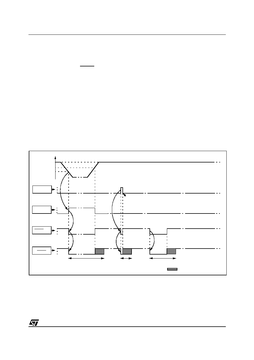
5.3 RESET
5.3.1 Introduction
The MCU can be reset in three ways:
s
A low pulse input on the RESET pin
s
Internal Watchdog reset
s
Internal Low Voltage Detector (LVD) reset
5.3.2 RESET Sequence
The basic RESET sequence consists of 3 main
phases:
s
Internal (watchdog or LVD) or external Reset
event
s
A delay of 2048 or 32768 clock (f
INT
) cycles
(selected through the option bytes)
s
RESET vector fetch
The reset delay allows the oscillator to stabilise
and ensures that recovery has taken place from
the Reset state.
The RESET vector fetch phase duration is 2 clock
cycles.
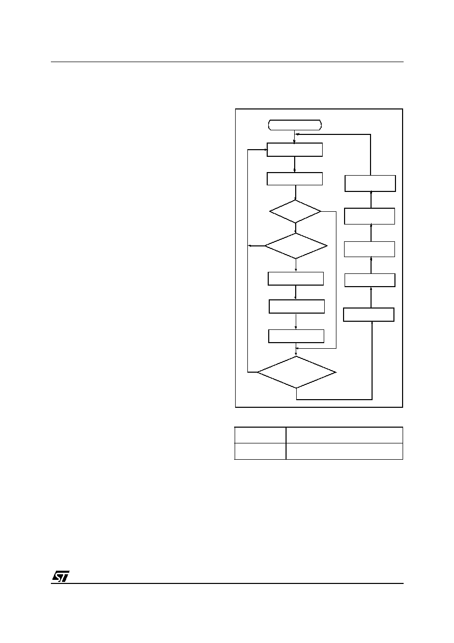
When a reset occurs:
≠ The stack is cleared
≠ The PC is loaded with the address of the Reset
vector. It is located in program ROM starting at
address 0FFEh.
A jump to the beginning of the user program must
be coded at this address.
≠ The interrupt flag is automatically set, so that the
CPU is in Non Maskable Interrupt mode. This
prevents the initialization routine from being in-
terrupted. The initialization routine should there-
fore be terminated by a RETI instruction, in order
to go back to normal mode.
Figure 13. RESET Sequence
V
DD
RESET PIN
WATCHDOG
V
IT+
V
IT-
WATCHDOG UNDERFLOW
RESET
2048 CLOCK CYCLE (fINT) DELAY
LVD
RESET
INTERNAL
RUN
RESET
RUN
RUN
RUN
RESET
RESET
RESET
1
ST6200C/ST6201C/ST6203C
24/100
RESET (Cont'd)
5.3.3 RESET Pin
The RESET pin may be connected to a device on
the application board in order to reset the MCU if
required. The RESET pin may be pulled low in
RUN, WAIT or STOP mode. This input can be
used to reset the internal state of the MCU and en-
sure it starts-up correctly. The pin, which is con-
nected to an internal pull-up, is active low and fea-
tures a Schmitt trigger input. A delay (2048 clock
cycles) added to the external signal ensures that
even short pulses on the RESET pin are accepted
as valid, provided V
DD
has completed its rising
phase and that the oscillator is running correctly
(normal RUN or WAIT modes). The MCU is kept in
the Reset state as long as the RESET pin is held
low.
If the RESET pin is grounded while the MCU is in
RUN or WAIT modes, processing of the user pro-
gram is stopped (RUN mode only), the I/O ports
are configured as inputs with pull-up resistors and
the main oscillator is restarted. When the level on
the RESET pin then goes high, the initialization se-
quence is executed at the end of the internal delay
period.
If the RESET pin is grounded while the MCU is in
STOP mode, the oscillator starts up and all the I/O
ports are configured as inputs with pull-up resis-
tors. When the RESET pin level then goes high,
the initialization sequence is executed at the end
of the internal delay period.
A simple external RESET circuitry is shown in
Fig-
ure 15
. For more details, please refer to the appli-
cation note AN669.
Figure 14. Reset Block Diagram
f
INT
COU
NTER
RESET
WATCHDOG RESET
LVD RESET
INTERNAL
RESET
R
ESD
1)
1) Resistive ESD protection.
V
DD
R
PU
20
48 o
r
3276
8
clock cycle
s
2)
2) The reset delay value is selected through the option bytes.
1
ST6200C/ST6201C/ST6203C
25/100
RESET (Cont'd)
5.3.4 Watchdog Reset
The MCU provides a Watchdog timer function in
order to be able to recover from software hang-
ups. If the Watchdog register is not refreshed be-
fore an end-of-count condition is reached, a
Watchdog reset is generated.
After a Watchdog reset, the MCU restarts in the
same way as if a Reset was generated by the RE-
SET pin.
Note: When a watchdog reset occurs, the RESET
pin is tied low for very short time period, to flag the
reset phase. This time is not long enough to reset
external circuits.
For more details refer to the Watchdog Timer
chapter.
5.3.5 LVD Reset
Two different RESET sequences caused by the in-
ternal LVD circuitry can be distinguished:
s
Power-On RESET
s
Voltage Drop RESET
During an LVD reset, the RESET pin is pulled low
when V
DD
<V
IT+
(rising edge) or V
DD
<V
IT-
(falling
edge).
For more details, refer to the LVD chapter.
Caution: Do not externally connect directly the
RESET pin to V
DD
, this may cause damage to the
component in case of internal RESET (Watchdog
or LVD).
Figure 15. Simple External Reset Circuitry
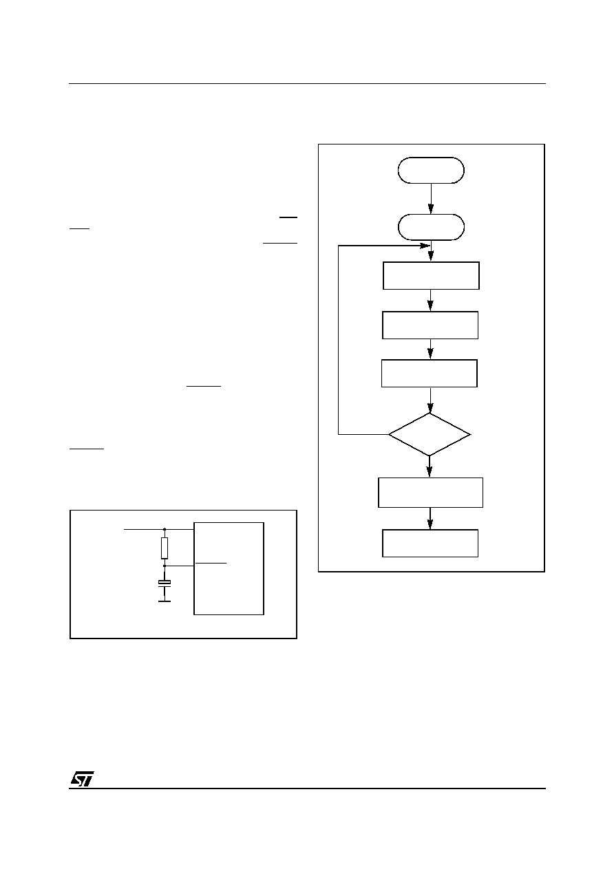
Figure 16. Reset Processing
ST62xx
RESET
V
DD
V
DD
R
C
Typical: R = 10K
C = 10nF
R > 4.7 K
INT LATCH CLEARED
NMI MASK SET
(IF PRESENT)
SELECT
NMI MODE FLAGS
IS RESET STILL
PRESENT?
YES
PUT FFEh
ON ADDRESS BUS
FROM RESET LOCATIONS
FFEh/FFFh
NO
FETCH INSTRUCTION
LOAD PC
INTERNAL
RESET
RESET
2048 OR 32768
CLOCK CYCLE
DELAY
1
ST6200C/ST6201C/ST6203C
26/100
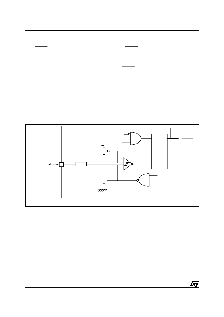
5.4 INTERRUPTS
The ST6 core may be interrupted by four maska-
ble interrupt sources, in addition to a Non Maska-
ble Interrupt (NMI) source. The interrupt process-
ing flowchart is shown in
Figure 18
.
Maskable interrupts must be enabled by setting
the GEN bit in the IOR register. However, even if
they are disabled (GEN bit = 0), interrupt events
are latched and may be processed as soon as the
GEN bit is set.
Each source is associated with a specific Interrupt
Vector, located in Program space (see
Table 7
). In
the vector location, the user must write a Jump in-
struction to the associated interrupt service rou-
tine.
When an interrupt source generates an interrupt
request, the PC register is loaded with the address
of the interrupt vector, which then causes a Jump
to the relevant interrupt service routine, thus serv-
icing the interrupt.
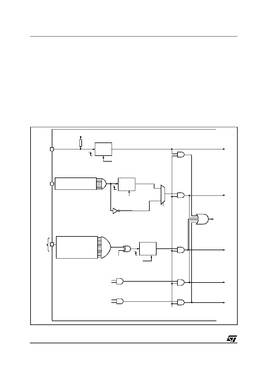
Interrupt are triggered by events either on external
pins, or from the on-chip peripherals. Several
events can be ORed on the same interrupt vector.
On-chip peripherals have flag registers to deter-
mine which event triggered the interrupt.
Figure 17. Interrupts Block Diagram
NMI
ESB BIT
VDD
LATCH
CLEARED BY H/W
AT START OF VECTOR #0 ROUTINE
VECTOR #0
LES BIT
1
0
LATCH
CLEARED BY H/W
AT START OF
VECTOR #1
VECTOR #2
VECTOR #3
VECTOR #4
LATCH
CLEARED
BY H/W AT START OF
VECTOR #2 ROUTINE
I/O PORT REGISTER
CONFIGURATION
"INPUT WITH INTERRUPT"
I/O PORT REGISTER
CONFIGURATION
"INPUT WITH INTERRUPT"
EXIT FROM
STOP/WAIT
VECTOR #1 ROUTINE
TIMER
A/D CONVERTER *
TMZ BIT
ETI BIT
EAI BIT
EOC BIT
GEN BIT
PB0..PB1
PA1..PA3
(TSCR REGISTER)
(ADCR REGISTER)
(IOR REGISTER)
(IOR REGISTER)
(IOR REGISTER)
PB3
PB5..PB7
* Depending on device. See device summary on page 1.
1

ST6200C/ST6201C/ST6203C
27/100
5.5 INTERRUPT RULES AND PRIORITY
MANAGEMENT
s
A Reset can interrupt the NMI and peripheral
interrupt routines
s
The Non Maskable Interrupt request has the
highest priority and can interrupt any peripheral
interrupt routine at any time but cannot interrupt
another NMI interrupt.
s
No peripheral interrupt can interrupt another. If
more than one interrupt request is pending,
these are processed by the processor core
according to their priority level: vector #1 has the
highest priority while vector #4 the lowest. The
priority of each interrupt source is fixed by
hardware (see
Interrupt Mapping table
).
5.6 INTERRUPTS AND LOW POWER MODES
All interrupts cause the processor to exit from
WAIT mode. Only the external and some specific
interrupts from the on-chip peripherals cause the
processor to exit from STOP mode (refer to the
"Exit from STOP" column in the Interrupt Mapping
Table).
5.7 NON MASKABLE INTERRUPT
This interrupt is triggered when a falling edge oc-
curs on the NMI pin regardless of the state of the
GEN bit in the IOR register. An interrupt request
on NMI vector #0 is latched by a flip flop which is
automatically reset by the core at the beginning of
the NMI service routine.
5.8 PERIPHERAL INTERRUPTS
Different peripheral interrupt flags in the peripheral
control registers are able to cause an interrupt
when they are active if both:
≠ The GEN bit of the IOR register is set
≠ The corresponding enable bit is set in the periph-
eral control register.
Peripheral interrupts are linked to vectors #3 and
#4. Interrupt requests are flagged by a bit in their
corresponding control register. This means that a
request cannot be lost, because the flag bit must
be cleared by user software.
1

ST6200C/ST6201C/ST6203C
28/100
5.9 EXTERNAL INTERRUPTS (I/O Ports)
External interrupt vectors can be loaded into the
PC register if the corresponding external interrupt
occurred and if the GEN bit is set. These interrupts
allow the processor to exit from STOP mode.
The external interrupt polarity is selected through
the IOR register.
External interrupts are linked to vectors #1 and #
2.
Interrupt requests on vector #1 can be configured
either as edge or level-sensitive using the LES bit
in the IOR Register.
Interrupt requests from vector #2 are always edge
sensitive. The edge polarity can be configured us-
ing the ESB bit in the IOR Register.
In edge-sensitive mode, a latch is set when a edge
occurs on the interrupt source line and is cleared
when the associated interrupt routine is started.
So, an interrupt request can be stored until com-
pletion of the currently executing interrupt routine,
before being processed. If several interrupt re-
quests occurs before completion of the current in-
terrupt routine, only the first request is stored.
Storing of interrupt requests is not possible in level
sensitive mode. To be taken into account, the low
level must be present on the interrupt pin when the
MCU samples the line after instruction execution.
5.9.1 Notes on using External Interrupts
ESB bit Spurious Interrupt on Vector #2
If a pin associated with interrupt vector #2 is con-
figured as interrupt with pull-up, whenever vector
#2 is configured to be rising edge sensitive (by set-
ting the ESB bit in the IOR register), an interrupt is
latched although a rising edge may not have oc-
cured on the associated pin.
This is due to the vector #2 circuitry.The worka-
round is to discard this first interrupt request in the
routine (using a flag for example).
Masking of One Interrupt by Another on Vector
#2.
When two or more port pins (associated with inter-
rupt vector #2) are configured together as input
with interrupt (falling edge sensitive), as long as
one pin is stuck at '0', the other pin can never gen-
erate an interrupt even if an active edge occurs at
this pin. The same thing occurs when one pin is
stuck at '1' and interrupt vector #2 is configured as
rising edge sensitive.
To avoid this the first pin must input a signal that
goes back up to '1' right after the falling edge. Oth-
erwise, in the interrupt routine for the first pin, de-
activate the "input with interrupt" mode using the
port control registers (DDR, OR, DR). An active
edge on another pin can then be latched.
I/O port Configuration Spurious Interrupt on
Vector #2
If a pin associated with interrupt vector #2 is in `in-
put with pull-up' state, a `0' level is present on the
pin and the ESB bit = 0, when the I/O pin is config-
ured as interrupt with pull-up by writing to the
DDRx, ORx and DRx register bits, an interrupt is
latched although a falling edge may not have oc-
curred on the associated pin.
In the opposite case, if the pin is in interrupt with
pull-up state , a 0 level is present on the pin and
the ESB bit =1, when the I/O port is configured as
input with pull-up by writing to the DDRx, ORx and
DRx bits, an interrupt is latched although a rising
edge may not have occurred on the associated
pin.
1
ST6200C/ST6201C/ST6203C
29/100
5.10 INTERRUPT HANDLING PROCEDURE
The interrupt procedure is very similar to a call pro-
cedure, in fact the user can consider the interrupt
as an asynchronous call procedure. As this is an
asynchronous event, the user cannot know the
context and the time at which it occurred. As a re-
sult, the user should save all Data space registers
which may be used within the interrupt routines.
The following list summarizes the interrupt proce-
dure:
When an interrupt request occurs, the following
actions are performed by the MCU automatically:
≠ The core switches from the normal flags to the
interrupt flags (or the NMI flags).
≠ The PC contents are stored in the top level of the
stack.
≠ The normal interrupt lines are inhibited (NMI still
active).
≠ The internal latch (if any) is cleared.
≠ The associated interrupt vector is loaded in the PC.
When an interrupt request occurs, the following
actions must be performed by the user software:
≠ User selected registers have to be saved within
the interrupt service routine (normally on a soft-
ware stack).
≠ The source of the interrupt must be determined
by polling the interrupt flags (if more than one
source is associated with the same vector).
≠ The RETI (RETurn from Interrupt) instruction
must end the interrupt service routine.
After the RETI instruction is executed, the MCU re-
turns to the main routine.
Caution: When a maskable interrupt occurs while
the ST6 core is in NORMAL mode and during the
execution of an "ldi IOR, 00h" instruction (disabling
all maskable interrupts): if the interrupt
request oc-
curs during the first 3 cycles of the "ldi" instruction
(which is a 4-cycle instruction) the core will switch
to interrupt mode BUT the flags CN and ZN will
NOT switch to the interrupt pair CI and ZI.
5.10.1 Interrupt Response Time
This is defined as the time between the moment
when the Program Counter is loaded with the in-
terrupt vector and when the program has jump to
the interrupt subroutine and is ready to execute
the code. It depends on when the interrupt occurs
while the core is processing an instruction.
Figure 18. Interrupt Processing Flow Chart
Table 6. Interrupt Response Time
One CPU cycle is 13 external clock cycles thus 11
CPU cycles = 11 x (13 /8M) = 17.875 µs with an 8
MHz external quartz.
Minimum
6 CPU cycles
Maximum
11 CPU cycles
INSTRUCTION
FETCH
INSTRUCTION
EXECUTE
INSTRUCTION
WAS
THE INSTRUCTION
A RETI ?
ENABLE
MASKABLE INTERRUPTS
SELECT
NORMAL FLAGS
"POP"
THE STACKED PC
IS THERE AN
AN INTERRUPT REQUEST
AND INTERRUPT MASK?
SELECT
INTERRUPT FLAGS
PUSH THE
PC INTO THE STACK
LOAD PC FROM
INTERRUPT VECTOR
DISABLE
MASKABLE INTERRUPT
NO
NO
YES
IS THE CORE
ALREADY IN
NORMAL MODE?
YES
NO
YES
CLEAR
INTERNAL LATCH
*)
*)
If a latch is present on the interrupt source line
1
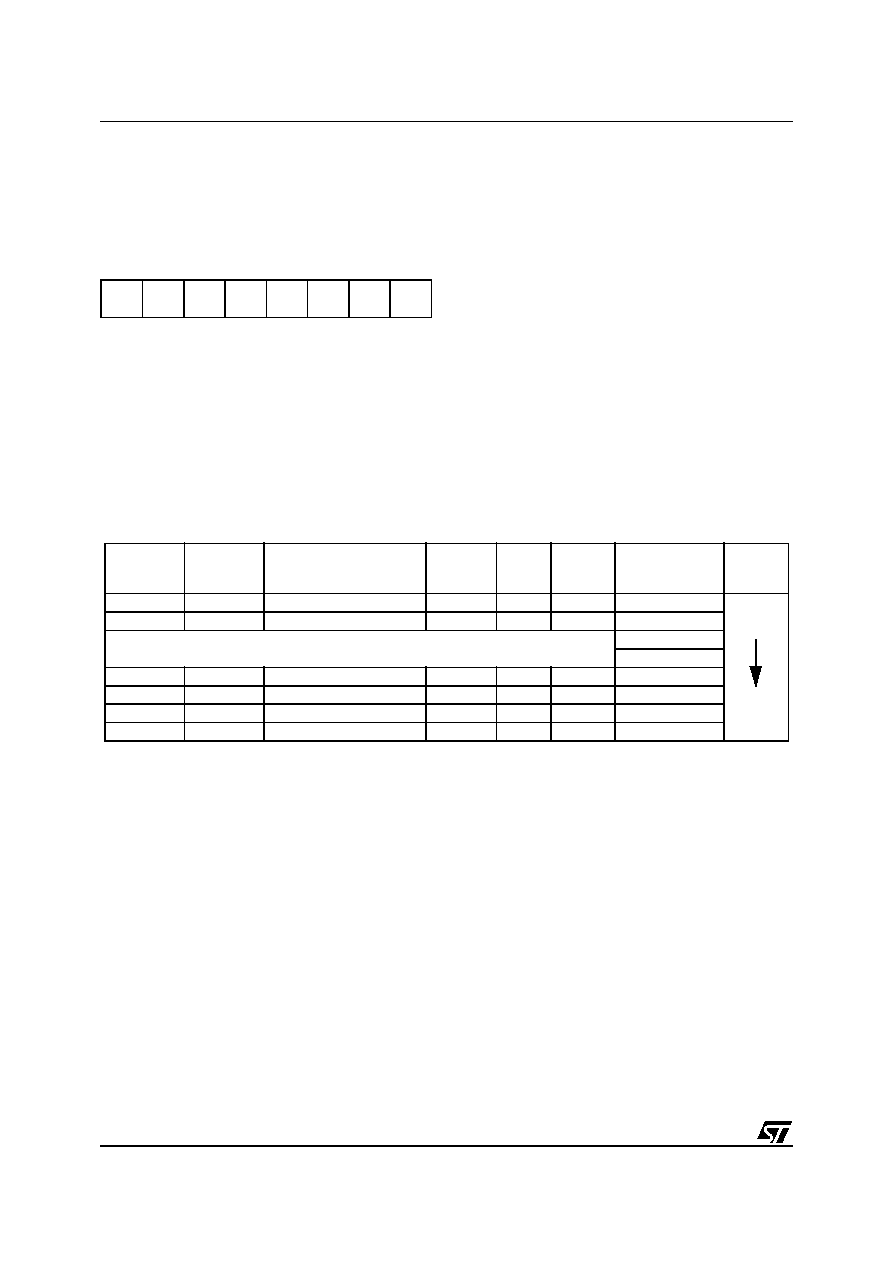
ST6200C/ST6201C/ST6203C
30/100
5.11 REGISTER DESCRIPTION
INTERRUPT OPTION REGISTER (IOR)
Address: 0C8h
--
Write Only
Reset status: 00h
Caution: This register is write-only and cannot be
accessed by single-bit operations (SET, RES,
DEC,...).
Bit 7 =Reserved, must be cleared.
Bit 6 = LES
Level/Edge Selection bit
.
0: Falling edge sensitive mode is selected for inter-
rupt vector #1
1: Low level sensitive mode is selected for inter-
rupt vector #1
Bit 5 = ESB
Edge Selection bit
.
0: Falling edge mode on interrupt vector #2
1: Rising edge mode on interrupt vector #2
Bit 4 = GEN
Global Enable Interrupt
.
0: Disable all maskable interrupts
1: Enable all maskable interrupts
Note: When the GEN bit is cleared, the NMI inter-
rupt is active but cannot be used to exit from STOP
or WAIT modes.
Bits 3:0 = Reserved, must be cleared.
Table 7. Interrupt Mapping
* Depending on device. See device summary on page 1.
7
0
-
LES
ESB
GEN
-
-
-
-
Vector
number
Source
Block
Description
Register
Label
Flag
Exit
from
STOP
Vector
Address
Priority
Order
RESET
Reset
N/A
N/A
yes
FFEh-FFFh
Vector #0
NMI
Non Maskable Interrupt
N/A
N/A
yes
FFCh-FFDh
NOT USED
FFAh-FFBh
FF8h-FF9h
Vector #1
Port A
Ext. Interrupt Port A
N/A
N/A
yes
FF6h-FF7h
Vector #2
Port B
Ext. Interrupt Port B
N/A
N/A
yes
FF4h-FF5h
Vector #3
TIMER
Timer underflow
TSCR
TMZ
yes
FF2h-FF3h
Vector #4
ADC *
End Of Conversion
ADCR
EOC
no
FF0h-FF1h
Priority
Lowest
Highest
Priority
1

ST6200C/ST6201C/ST6203C
31/100
6 POWER SAVING MODES
6.1 INTRODUCTION
To give a large measure of flexibility to the applica-
tion in terms of power consumption, two main pow-
er saving modes are implemented in the ST6 (see
Figure 19
).
In addition, the Low Frequency Auxiliary Oscillator
(LFAO) can be used instead of the main oscillator
to reduce power consumption in RUN and WAIT
modes.
After a RESET the normal operating mode is se-
lected by default (RUN mode). This mode drives
the device (CPU and embedded peripherals) by
means of a master clock which is based on the
main oscillator frequency.
From Run mode, the different power saving
modes may be selected by calling the specific ST6
software instruction or for the LFAO by setting the
relevant register bit. For more information on the
LFAO, please refer to the Clock chapter.
Figure 19. Power Saving Mode Transitions
POWER CONSUMPTION
WAIT
LFAO
RUN
STOP
High
Low
1

ST6200C/ST6201C/ST6203C
32/100
6.2 WAIT MODE
The MCU goes into WAIT mode as soon as the
WAIT instruction is executed. This has the follow-
ing effects:
≠ Program execution is stopped, the microcontrol-
ler software can be considered as being in a "fro-
zen" state.
≠ RAM contents and peripheral registers are pre-
served as long as the power supply voltage is
higher than the RAM retention voltage.
≠ The oscillator is kept running to provide a clock
to the peripherals; they are still active.
WAIT mode can be used when the user wants to
reduce the MCU power consumption during idle
periods, while not losing track of time or the ability
to monitor external events. WAIT mode places the
MCU in a low power consumption mode by stop-
ping the CPU. The active oscillator (main oscillator
or LFAO) is kept running in order to provide a clock
signal to the peripherals.
If the power consumption has to be further re-
duced, the Low Frequency Auxiliary Oscillator
(LFAO) can be used in place of the main oscillator,
if its operating frequency is lower. If required, the
LFAO must be switched on before entering WAIT
mode.
Exit from Wait mode
The MCU remains in WAIT mode until one of the
following events occurs:
≠ RESET (Watchdog, LVD or RESET pin)
≠ A peripheral interrupt (timer, ADC,...),
≠ An external interrupt (I/O port, NMI)
The Program Counter then branches to the start-
ing address of the interrupt or RESET service rou-
tine. Refer to
Figure 20
.
See also
Section 6.4.1
.
Figure 20. WAIT Mode Flowchart
WAIT INSTRUCTION
RESET
INTERRUPT
Y
N
N
Y
Clock to CPU
OSCILLATOR
Clock to PERIPHERALS
On
Yes
No
FETCH RESET VECTOR
OR SERVICE INTERRUPT
2048 OR 32768
Clock to CPU
OSCILLATOR
Clock to PERIPHERALS
Restart
Yes
Yes
DELAY
CLOCK CYCLE
OSCILLATOR
Clock to PERIPHERALS
Clock to CPU
Yes
Yes
On
1
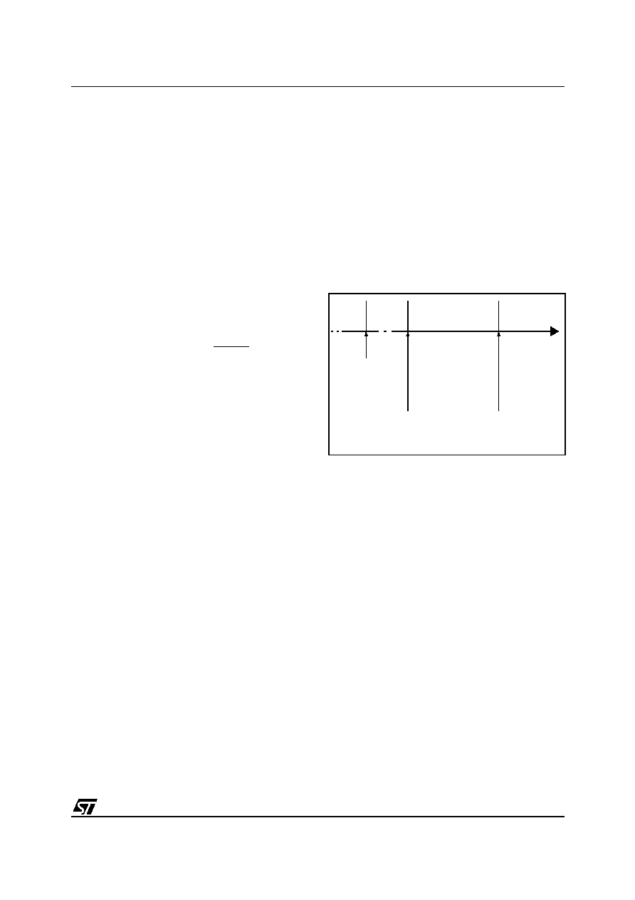
ST6200C/ST6201C/ST6203C
33/100
6.3 STOP MODE
STOP mode is the lowest power consumption
mode of the MCU (see
Figure 22
).
The MCU goes into STOP mode as soon as the
STOP instruction is executed. This has the follow-
ing effects:
≠ Program execution is stopped, the microcontrol-
ler can be considered as being "frozen".
≠ The contents of RAM and the peripheral regis-
ters are kept safely as long as the power supply
voltage is higher than the RAM retention voltage.
≠ The oscillator is stopped, so peripherals cannot
work except the those that can be driven by an
external clock.
Exit from STOP Mode
The MCU remains in STOP mode until one of the
following events occurs:
≠ RESET (Watchdog, LVD or RESET pin)
≠ A peripheral interrupt (assuming this peripheral
can be driven by an external clock)
≠ An external interrupt (I/O port, NMI)
In all cases a delay of 2048 or 32768 clock cycles
(f
INT
) is generated to make sure the oscillator has
started properly.
The Program Counter then points to the starting
address of the interrupt or RESET service routine
(see
Figure 21
).
STOP Mode and Watchdog
When the Watchdog is active (hardware or soft-
ware activation), the STOP instruction is disabled
and a WAIT instruction will be executed in its place
unless the EXCTNL option bit is set to 1 in the op-
tion bytes and a a high level is present on the NMI
pin. In this case, the STOP instruction will be exe-
cuted and the Watchdog will be frozen.
Figure 21. STOP Mode Timing Overview
STOP
RUN
RUN
2048 or 32768
RESET
OR
INTERRUPT
STOP
INSTRUCTION
FETCH
VECTOR
CYCLE
CLOCK
DELAY
1
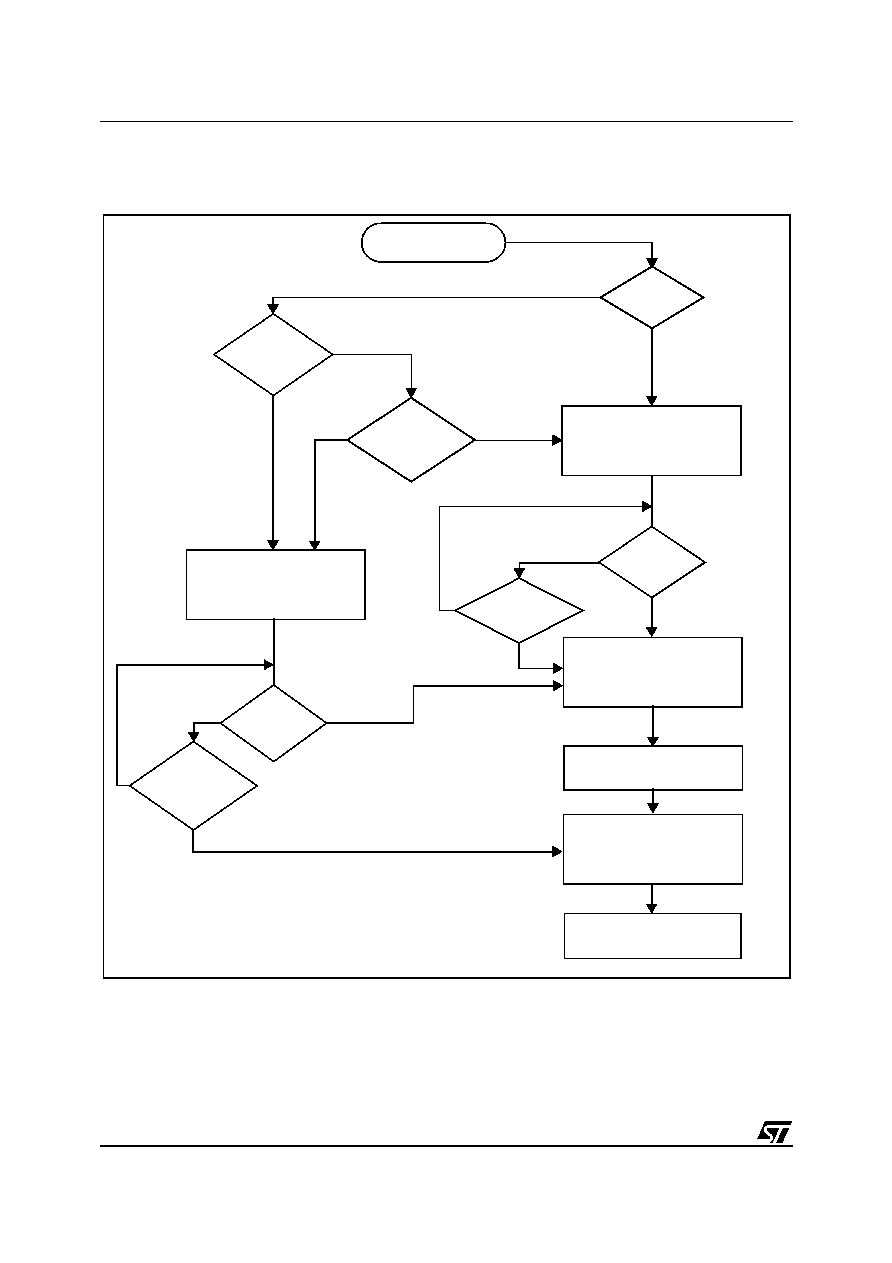
ST6200C/ST6201C/ST6203C
34/100
STOP MODE (Cont'd)
Figure 22. STOP Mode Flowchart
Notes:
1. EXCTNL is an option bit. See option byte section for more details.
2. Peripheral clocked with an external clock source can still be active.
3. Only some specific interrupts can exit the MCU from STOP mode (such as external interrupt). Refer to
the Interrupt Mapping table for more details.
STOP INSTRUCTION
RESET
INTERRUPT
3)
Y
N
N
Y
FETCH RESET VECTOR
OR SERVICE INTERRUPT
WATCHDOG
ENABLE
DISABLE
EXCTNL
1
1
LEVEL
ON
NMI PIN
0
0
RESET
INTERRUPT
N
N
Y
Y
VALUE
1)
Clock to CPU
OSCILLATOR
Clock to PERIPHERALS
2)
Off
No
No
2048 or 32768
DELAY
Clock to CPU
OSCILLATOR
Clock to PERIPHERALS
Restart
Yes
Yes
Clock to CPU
OSCILLATOR
Clock to PERIPHERALS
On
Yes
Yes
Clock to CPU
OSCILLATOR
Clock to PERIPHERALS
On
Yes
No
CLOCK CYCLE
1

ST6200C/ST6201C/ST6203C
35/100
6.4 NOTES RELATED TO WAIT AND STOP MODES
6.4.1 Exit from Wait and Stop Modes
6.4.1.1 NMI Interrupt
It should be noted that when the GEN bit in the
IOR register is low (interrupts disabled), the NMI
interrupt is active but cannot cause a wake up from
STOP/WAIT modes.
6.4.1.2 Restart Sequence
When the MCU exits from WAIT or STOP mode, it
should be noted that the restart sequence de-
pends on the original state of the MCU (normal, in-
terrupt or non-maskable interrupt mode) prior to
entering WAIT or STOP mode, as well as on the
interrupt type.
Normal Mode. If the MCU was in the main routine
when the WAIT or STOP instruction was execut-
ed, exit from Stop or Wait mode will occur as soon
as an interrupt occurs; the related interrupt routine
is executed and, on completion, the instruction
which follows the STOP or WAIT instruction is
then executed, providing no other interrupts are
pending.
Non Maskable Interrupt Mode. If the STOP or
WAIT instruction has been executed during execu-
tion of the non-maskable interrupt routine, the
MCU exits from Stop or Wait mode as soon as an
interrupt occurs: the instruction which follows the
STOP or WAIT instruction is executed, and the
MCU remains in non-maskable interrupt mode,
even if another interrupt has been generated.
Normal Interrupt Mode. If the MCU was in inter-
rupt mode before the STOP or WAIT instruction
was executed, it exits from STOP or WAIT mode
as soon as an interrupt occurs. Nevertheless, two
cases must be considered:
≠ If the interrupt is a normal one, the interrupt rou-
tine in which the WAIT or STOP mode was en-
tered will be completed, starting with the
execution of the instruction which follows the
STOP or the WAIT instruction, and the MCU is
still in interrupt mode. At the end of this routine
pending interrupts will be serviced according to
their priority.
≠ In the event of a non-maskable interrupt, the
non-maskable interrupt service routine is proc-
essed first, then the routine in which the WAIT or
STOP mode was entered will be completed by
executing the instruction following the STOP or
WAIT instruction. The MCU remains in normal in-
terrupt mode.
6.4.2 Recommended MCU Configuration
For lowest power consumption during RUN or
WAIT modes, the user software must configure
the MCU as follows:
≠ Configure unused I/Os as output push-pull low
mode
≠ Place all peripherals in their power down modes
before entering STOP mode
≠ Select the Low Frequency Auxiliary Oscillator
(provided this runs at a lower frequency than the
main oscillator).
The WAIT and STOP instructions are not execut-
ed if an enabled interrupt request is pending.
1

ST6200C/ST6201C/ST6203C
36/100
7 I/O PORTS
7.1 INTRODUCTION
Each I/O port contains up to 8 pins. Each pin can
be programmed independently as digital input
(with or without pull-up and interrupt generation),
digital output (open drain, push-pull) or analog in-
put (when available).
The I/O pins can be used in either standard or al-
ternate function mode.
Standard I/O mode is used for:
≠ Transfer of data through digital inputs and out-
puts (on specific pins):
≠ External interrupt generation
Alternate function mode is used for:
≠ Alternate signal input/output for the on-chip
peripherals
The generic I/O block diagram is shown in
Figure
23
.
7.2 FUNCTIONAL DESCRIPTION
Each port is associated with 3 registers located in
Data space:
≠ Data Register (DR)
≠ Data Direction Register (DDR)
≠ Option Register (OR)
Each I/O pin may be programmed using the corre-
sponding register bits in the DDR, DR and OR reg-
isters: bit x corresponding to pin x of the port.
Table
8
illustrates the various port configurations which
can be selected by user software.
During MCU initialization, all I/O registers are
cleared and the input mode with pull-up and no in-
terrupt generation is selected for all the pins, thus
avoiding pin conflicts.
7.2.1 Digital Input Modes
The input configuration is selected by clearing the
corresponding DDR register bit.
In this case, reading the DR register returns the
digital value applied to the external I/O pin.
Different input modes can be selected by software
through the DR and OR registers, see
Table 8
.
External Interrupt Function
All input lines can be individually connected by
software to the interrupt system by programming
the OR and DR registers accordingly. The inter-
rupt trigger modes (falling edge, rising edge and
low level) can be configured by software for each
port as described in the Interrupt section.
7.2.2 Analog Inputs
Some pins can be configured as analog inputs by
programming the OR and DR registers according-
ly, see
Table 8
. These analog inputs are connect-
ed to the on-chip 8-bit Analog to Digital Converter.
Caution: ONLY ONE
pin should be programmed
as an analog input at any time, since by selecting
more than one input simultaneously their pins will
be effectively shorted.
7.2.3 Output Modes
The output configuration is selected by setting the
corresponding DDR register bit. In this case, writ-
ing to the DR register applies this digital value to
the I/O pin through the latch. Then, reading the DR
register returns the previously stored value.
Two different output modes can be selected by
software through the OR register: push-pull and
open-drain.
DR register value and output pin status:
Note: The open drain setting is not a true open
drain. This means it has the same structure as the
push-pull setting but the P-buffer is deactivated.
To avoid damaging the device, please respect the
V
OUT
absolute maximum rating described in the
Electrical Characteristics section.
7.2.4 Alternate Functions
When an on-chip peripheral is configured to use a
pin, the alternate function (timer input/output...) is
not systematically selected but has to be config-
ured through the DDR, OR and DR registers. Re-
fer to the chapter describing the peripheral for
more details.
DR
Push-pull
Open-drain
0
V
SS
V
SS
1
V
DD
Floating
1
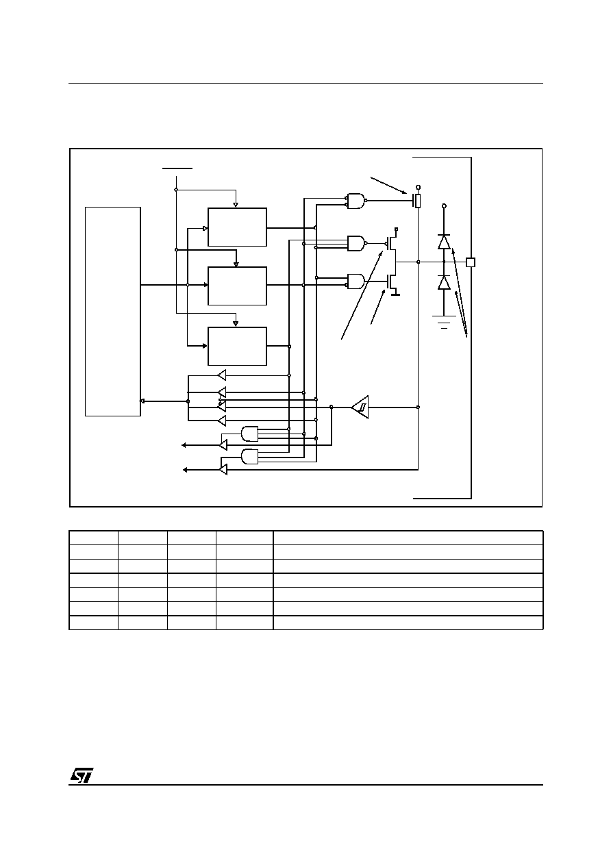
ST6200C/ST6201C/ST6203C
37/100
I/O PORTS (Cont'd)
Figure 23. I/O Port Block Diagram
Table 8. I/O Port Configurations
Note: x = Don't care
DDR
OR
DR
Mode
Option
0
0
0
Input
With pull-up, no interrupt
0
0
1
Input
No pull-up, no interrupt
0
1
0
Input
With pull-up and with interrupt
0
1
1
Input
Analog input (when available)
1
0
x
Output
Open-drain output (20mA sink when available)
1
1
x
Output
Push-pull output (20mA sink when available)
V
DD
RESET
ST6
INTERNAL
DATA
DATA
DIRECTION
REGISTER
REGISTER
OPTION
REGISTER
TO INTERRUPT
V
DD
TO ADC
V
DD
N-BUFFER
P-BUFFER
PULL-UP
CMOS
SCHMITT
TRIGGER
Pxx I/O Pin
BUS
CLAMPING
DIODES
*
* Depending on device. See device summary on page 1
.
1
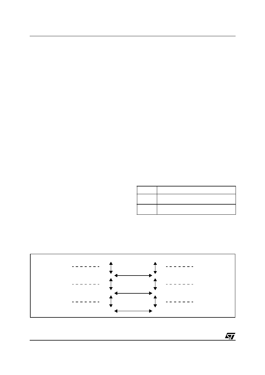
ST6200C/ST6201C/ST6203C
38/100
I/O PORTS (Cont'd)
7.2.5 Instructions NOT to be used to access
Port Data registers (SET, RES, INC and DEC)
DO NOT USE READ-MODIFY-WRITE INSTRUC-
TIONS (SET, RES, INC and DEC) ON PORT
DATA REGISTERS IF ANY PIN OF THE PORT IS
CONFIGURED IN INPUT MODE.
These instructions make an implicit read and write
back of the entire register. In port input mode,
however, the data register reads from the input
pins directly, and not from the data register latch-
es. Since data register information in input mode is
used to set the characteristics of the input pin (in-
terrupt, pull-up, analog input), these may be unin-
tentionally reprogrammed depending on the state
of the input pins.
As a general rule, it is better to only use single bit
instructions on data registers when the whole (8-
bit) port is in output mode. In the case of inputs or
of mixed inputs and outputs, it is advisable to keep
a copy of the data register in RAM. Single bit in-
structions may then be used on the RAM copy, af-
ter which the whole copy register can be written to
the port data register:
SET bit, datacopy
LD a, datacopy
LD DRA, a
7.2.6 Recommendations
1. Safe I/O State Switching Sequence
Switching the I/O ports from one state to another
should be done in a sequence which ensures that
no unwanted side effects can occur. The recom-
mended safe transitions are illustrated in
Figure 24
The Interrupt Pull-up to Input Analog transition
(and vice-vesra) is potentially risky and should be
avoided when changing the I/O operating mode.
2. Handling Unused Port Bits
On ports that have less than 8 external pins con-
nected:
≠ Leave the unbonded pins in reset state and do
not change their configuration.
≠ Do not use instructions that act on a whole port
register (INC, DEC, or read operations). Unavail-
able bits must be masked by software (AND in-
struction). Thus, when a read operation
performed on an incomplete port is followed by a
comparison, use a mask.
3. High Impedance Input
On any CMOS device, it is not recommended to
connect high impedance on input pins. The choice
of these impedance has to be done with respect to
the maximum leakage current defined in the da-
tasheet. The risk is to be close or out of specifica-
tion on the input levels applied to the device.
7.3 LOW POWER MODES
The WAIT and STOP instructions allow the
ST62xx to be used in situations where low power
consumption is needed. The lowest power con-
sumption is achieved by configuring I/Os in output
push-pull low mode.
7.4 INTERRUPTS
The external interrupt event generates an interrupt
if the corresponding configuration is selected with
DDR, DR and OR registers (see
Table 8
) and the
GEN-bit in the IOR register is set.
Figure 24. Diagram showing Safe I/O State Transitions
Note *. xxx = DDR, OR, DR Bits respectively
Mode Description
WAIT
No effect on I/O ports. External interrupts
cause the device to exit from WAIT mode.
STOP
No effect on I/O ports. External interrupts
cause the device to exit from STOP mode.
Interrupt
pull-up
Output
Open Drain
Output
Push-pull
Input
pull-up (Reset
state)
Input
Analog
Output
Open Drain
Output
Push-pull
Input
010*
000
100
110
011
001
101
111
1
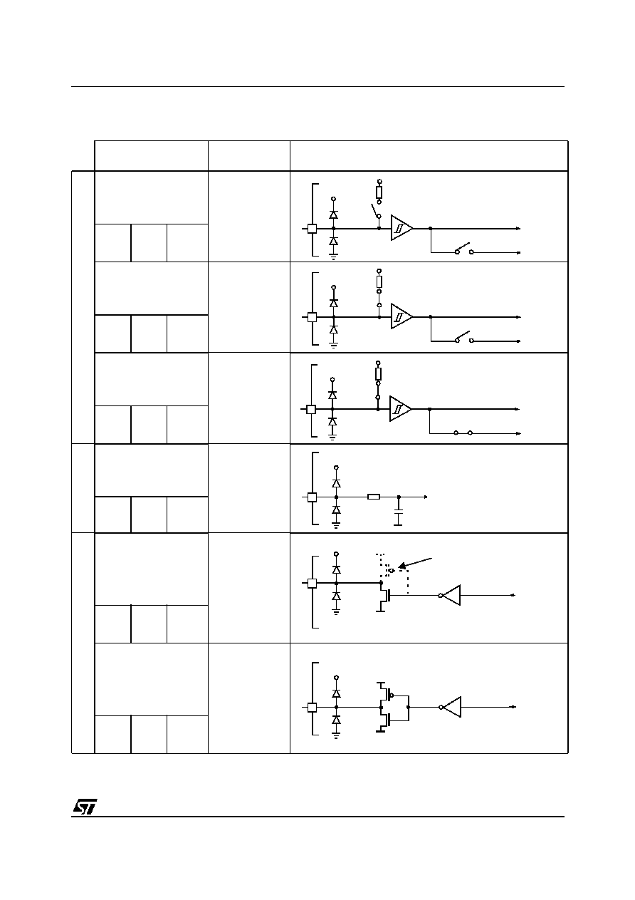
ST6200C/ST6201C/ST6203C
39/100
I/O PORTS (Cont'd)
Table 9. I/O Port Option Selections
Note 1. Provided the correct configuration has been selected (see
Table 8
).
MODE
AVAILABLE ON
(1)
SCHEMATIC
Digita
l Inp
ut
Input
PA1-PA3
PB0, PB1, PB3,
PB5-PB7
DDRx
0
ORx
0
DRx
1
Reset state
Input
with pull up
PA1-PA3
PB0, PB1, PB3,
PB5-PB7
DDRx
0
ORx
0
DRx
0
Input
with pull up
with interrupt
PA1-PA3
PB0, PB1, PB3,
PB5-PB7
DDRx
0
ORx
1
DRx
0
An
alog
Input
Analog Input
PB3, PB5-PB7
(Except on
ST6203C)
DDRx
0
ORx
1
DRx
1
D
igital
outp
ut
Open drain output (5mA)
Open drain output (20 mA)
PB0, PB1, PB3,
PB5-PB7
PA1-PA3
DDRx
1
ORx
0
DRx
0/1
Push-pull output (5mA)
Push-pull output (20 mA)
PB0, PB1, PB3,
PB5-PB7
PA1-PA3
DDRx
1
ORx
1
DRx
0/1
Data in
Interrupt
V
DD
V
DD
Data in
Interrupt
V
DD
V
DD
Data in
Interrupt
V
DD
V
DD
ADC
V
DD
Data out
P-buffer disconnected
V
DD
Data out
V
DD
1
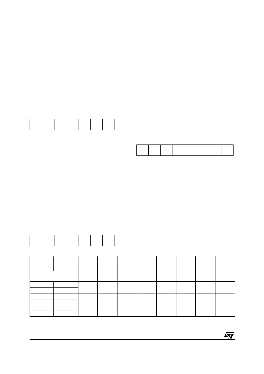
ST6200C/ST6201C/ST6203C
40/100
I/O PORTS (Cont'd)
7.5 REGISTER DESCRIPTION
DATA REGISTER (DR)
Port x Data Register
DRx with x = A or B.
Address DRA: 0C0h - Read /Write
Address DRB: 0C1h - Read /Write
Reset Value: 0000 0000 (00h)
Bit 7:0 = D[7:0]
Data register bits.
Reading the DR register returns either the DR reg-
ister latch content (pin configured as output) or the
digital value applied to the I/O pin (pin configured
as input).
Caution: In input mode, modifying this register will
modify the I/O port configuration (see
Table 8
).
Do not use the Single bit instructions on I/O port
data registers. See (
Section 7.2.5
).
DATA DIRECTION REGISTER (DDR)
Port x Data Direction Register
DDRx with x = A or B.
Address DDRA: 0C4h - Read /Write
Address DDRB: 0C5h - Read /Write
Reset Value: 0000 0000 (00h)
Bit 7:0 = DD[7:0]
Data direction register bits.
The DDR register gives the input/output direction
configuration of the pins. Each bit is set and
cleared by software.
0: Input mode
1: Output mode
OPTION REGISTER (OR)
Port x Option Register
ORx with x = A or B.
Address ORA: 0CCh - Read/Write
Address ORB: 0CDh - Read/Write
Reset Value: 0000 0000 (00h)
Bit 7:0 = O[7:0]
Option register bits.
The OR register allows to distinguish in output
mode if the push-pull or open drain configuration is
selected.
Output mode:
0: Open drain output(with P-Buffer deactivated)
1: Push-pull Output
Input mode: See
Table 8
.
Each bit is set and cleared by software.
Caution: Modifying this register, will also modify
the I/O port configuration in input mode. (see
Ta-
ble 8
).
Table 10. I/O Port Register Map and Reset Values
7
0
D7
D6
D5
D4
D3
D2
D1
D0
7
0
DD7
DD6
DD5
DD4
DD3
DD2
DD1
DD0
7
0
O7
O6
O5
O4
O3
O2
O1
O0
Address
(Hex.)
Register
Label
7
6
5
4
3
2
1
0
Reset Value
of all I/O port registers
0
0
0
0
0
0
0
0
0C0h
DRA
MSB
LSB
0C1h
DRB
0C4h
DDRA
MSB
LSB
0C5h
DDRB
0CCh
ORA
MSB
LSB
0CDh
ORB
1
ST6200C/ST6201C/ST6203C
41/100
8 ON-CHIP PERIPHERALS
8.1 WATCHDOG TIMER (WDG)
8.1.1 Introduction
The Watchdog timer is used to detect the occur-
rence of a software fault, usually generated by ex-
ternal interference or by unforeseen logical condi-
tions, which causes the application program to
abandon its normal sequence. The Watchdog cir-
cuit generates an MCU reset on expiry of a pro-
grammed time period, unless the program refresh-
es the counter's contents before the SR bit be-
comes cleared.
8.1.2 Main Features
s
Programmable timer (64 steps of 3072 clock
cycles)
s
Software reset
s
Reset (if watchdog activated) when the SR bit
reaches zero
s
Hardware or software watchdog activation
selectable by option bit (Refer to the option
bytes section)
Figure 25. Watchdog Block Diagram
RESET
C
7-BIT DOWNCOUNTER
f
int /12
SR
T0
CLOCK DIVIDER
WATCHDOG REGISTER (WDGR)
˜
256
T1
T2
T3
T4
T5
bit 0
bit 7
1
ST6200C/ST6201C/ST6203C
42/100
WATCHDOG TIMER (Cont'd)
8.1.3 Functional Description
The watchdog activation is selected through an
option in the option bytes:
≠ HARDWARE Watchdog option
After reset, the watchdog is permanently active,
the C bit in the WDGR is forced high and the user
can not change it. However, this bit can be read
equally as 0 or 1.
≠ SOFTWARE Watchdog option
After reset, the watchdog is deactivated. The func-
tion is activated by setting C bit in the WDGR reg-
ister. Once activated, it cannot be deactivated.
The counter value stored in the WDGR register
(bits SR:T0), is decremented every 3072 clock cy-
cles. The length of the timeout period can be pro-
grammed by the user in 64 steps of 3072 clock cy-
cles.
If the watchdog is activated (by setting the C bit)
and when the SR bit is cleared,
the watchdog initi-
ates a reset cycle pulling the reset pin low for typi-
cally 500ns.
The application program must write in the WDGR
register at regular intervals during normal opera-
tion to prevent an MCU reset. The value to be
stored in the WDGR register must be between
FEh and 02h (see
Table 11
). To run the watchdog
function the following conditions must be true:
≠ The C bit is set (watchdog activated)
≠ The SR bit is set to prevent generating an imme-
diate reset
≠ The T[5:0] bits contain the number of decre-
ments which represent the time delay before the
watchdog produces a reset.
Table 11. Watchdog Timing (f
OSC
= 8 MHz)
8.1.3.1 Software Reset
The SR bit can be used to generate a software re-
set by clearing the SR bit while the C bit is set.
8.1.4 Recommendations
1. The Watchdog plays an important supporting
role in the high noise immunity of ST62xx devices,
and should be used wherever possible. Watchdog
related options should be selected on the basis of
a trade-off between application security and STOP
mode availability (refer to the description of the
WDACT and EXTCNTL bits on the Option Bytes).
When STOP mode is not required, hardware acti-
vation without EXTERNAL STOP MODE CON-
TROL should be preferred, as it provides maxi-
mum security, especially during power-on.
When STOP mode is required, hardware activa-
tion and EXTERNAL STOP MODE CONTROL
should be chosen. NMI should be high by default,
to allow STOP mode to be entered when the MCU
is idle.
The NMI pin can be connected to an I/O line (see
Figure 26
) to allow its state to be controlled by soft-
ware. The I/O line can then be used to keep NMI
low while Watchdog protection is required, or to
avoid noise or key bounce. When no more
processing is required, the I/O line is released and
the device placed in STOP mode for lowest power
consumption.
Figure 26. A typical circuit making use of the
EXERNAL STOP MODE CONTROL feature
2. When software activation is selected (WDACT
bit in Option byte) and the Watchdog is not activat-
ed, the downcounter may be used as a simple 7-
bit timer (remember that the bits are in reverse or-
der).
The software activation option should be chosen
only when the Watchdog counter is to be used as
a timer. To ensure the Watchdog has not been un-
expectedly activated, the following instructions
should be executed:
jrr 0, WDGR, #+3 ; If C=0,jump to next
ldi WDGR, 0FDH
; SR=0 -> reset
next :
WDGR Register
initial value
WDG timeout period
(ms)
Max.
FEh
24.576
Min.
02h
0.384
NMI
SWITCH
I/O
VR02002
1

ST6200C/ST6201C/ST6203C
43/100
WATCHDOG TIMER (Cont'd)
These instructions test the C bit and reset the
MCU (i.e. disable the Watchdog) if the bit is set
(i.e. if the Watchdog is active), thus disabling the
Watchdog.
For more information on the use of the watchdog,
please read application note AN1015.
Note: This note applies only when the watchdog is
used as a standard timer. It is recommended to
read the counter twice, as it may sometimes return
an invalid value if the read is performed while the
counter is decremented (counter bits in transient
state). To validate the return value, both values
read must be equal. The counter decrements eve-
ry 384 µs at 8 MHz f
OSC
.
8.1.5 Low Power Modes
8.1.6 Interrupts
None.
Mode Description
WAIT
No effect on Watchdog.
STOP
Behaviour depends on the EXTCNTL option in the Option bytes:
1. Watchdog disabled:
The MCU will enter Stop mode if a STOP instruction is executed.
2. Watchdog enabled and EXTCNTL option disabled:
If a STOP instruction is encountered, it is interpreted as a WAIT.
3. Watchdog and EXTCNTL option enabled:
If a STOP instruction is encountered when the NMI pin is low, it is interpreted as a WAIT. If, however, the
STOP instruction is encountered when the NMI pin is high, the Watchdog counter is frozen and the CPU en-
ters STOP mode.
When the MCU exits STOP mode (i.e. when an interrupt is generated), the Watchdog resumes its activity.
1

ST6200C/ST6201C/ST6203C
44/100
WATCHDOG TIMER (Cont'd)
8.1.7 Register Description
WATCHDOG REGISTER (WDGR)
Address: 0D8h - Read /Write
Reset Value: 1111 1110 (FE h)
Bits 7:2 = T[5:0]
Downcounter bits
Caution: These bits are reversed and shifted with
respect to the physical counter: bit-7 (T0) is the
LSB of the Watchdog downcounter and bit-2 (T5)
is the MSB.
Bit 1 = SR:
Software Reset bit
Software can generate a reset by clearing this bit
while the C bit is set. When C = 0 (Watchdog de-
activated) the SR bit is the MSB of the 7-bit timer.
0: Generate (write)
1: No software reset generated, MSB of 7-bit timer
Bit 0 = C
Watchdog Control bit
.
If the hardware option is selected (WDACT bit in
Option byte), this bit is forced high and cannot be
changed by the user (the Watchdog is always ac-
tive). When the software option is selected
(WDACT bit in Option byte), the Watchdog func-
tion is activated by setting the C bit, and cannot
then be deactivated (except by resetting the
MCU).
When C is kept cleared the counter can be used
as a 7-bit timer.
0: Watchdog deactivated
1: Watchdog activated
7
0
T0
T1
T2
T3
T4
T5
SR
C
1
ST6200C/ST6201C/ST6203C
45/100
8.2 8-BIT TIMER
8.2.1 Introduction
The 8-Bit Timer on-chip peripheral is a free run-
ning downcounter based on an 8-bit downcounter
with a 7-bit programmable prescaler, giving a max-
imum count of 2
15
.
8.2.2 Main Features
s
Time-out downcounting mode with up to 15-bit
accuracy
s
Interrupt capability on counter underflow
The timer can be used in WAIT mode to wake up
the MCU.
Figure 27. Timer Block Diagram
INTERRUPT
TMZ
ETI
TSCR5 TSCR4
PSI
PS2
PS1
PS0
TSCR
PROGRAMMABLE PRESCALER
PSCR6 PSCR5 PSCR4 PSCR3 PSCR2 PSCR1 PSCR0
PSCR REGISTER
0
7
0
TCR7
TCR6
TCR5
TCR4
TCR3
TCR2
TCR1
TCR0
TCR
7
0
RE
L
O
A
D
8-BIT DOWN COUNTER
f
PRESCALER
f
COUNTER
f
INT/12
PSCR7
7
/2
/1
/4
/8
/16
/32
/64
/128
REGISTER
REGISTER
1

ST6200C/ST6201C/ST6203C
46/100
8-BIT TIMER (Cont'd)
8.2.3 Counter/Prescaler Description
Prescaler
The prescaler input is the internal frequency f
INT
divided by 12. The prescaler decrements on the
rising edge, depending on the division factor pro-
grammed by the PS[2:0] bits in the TSCR register.
The state of the 7-bit prescaler can be read in the
PSCR register.
When the prescaler reaches 0, it is automatically
reloaded with 7Fh.
Counter
The free running 8-bit downcounter is fed by the
output of the programmable prescaler, and is dec-
remented on every rising edge of the f
COUNTER
clock signal coming from the prescaler.
It is possible to read or write the contents of the
counter on the fly, by reading or writing the timer
counter register (TCR).
When the downcounter reaches 0, it is automati-
cally reloaded with the value 0FFh.
Counter Clock and Prescaler
The counter clock frequency is given by:
f
COUNTER
= f
PRESCALER
/ 2
PS[2:0]
where f
PRESCALER
is:
≠ f
INT
/12
The timer input clock feeds the 7-bit programma-
ble prescaler. The prescaler output can be pro-
grammed by selecting one of the 8 available pres-
caler taps using the PS[2:0] bits in the Status/Con-
trol Register (TSCR). Thus the division factor of
the prescaler can be set to 2
n
(where n equals 0, to
7). See
Figure 27
.
The clock input is enabled by the PSI (Prescaler
Initialize) bit in the TSCR register. When PSI is re-
set, the counter is frozen and the prescaler is load-
ed with the value 7Fh. When PSI is set, the pres-
caler and the counter run at the rate of the select-
ed clock source.
Counter and Prescaler Initialization
After RESET, the counter and the prescaler are in-
itialized to 0FFh and 7Fh respectively.
The 7-bit prescaler can be initialized to 7Fh by
clearing the PSI bit. Direct write access to the
prescaler is also possible when PSI =1. Then, any
value between 0 and 7Fh can be loaded into it.
The 8-bit counter can be initialized separately by
writing to the TCR register.
8.2.3.1 8-bit Counting and Interrupt Capability
on Counter Underflow
Whatever the division factor defined for the pres-
caler, the Timer Counter works as an 8-bit down-
counter. The input clock frequency is user selecta-
ble using the PS[2:0] bits.
When the downcounter decrements to zero, the
TMZ (Timer Zero) bit in the TSCR is set. If the ETI
(Enable Timer Interrupt) bit in the TSCR is also
set, an interrupt request is generated.
The Timer interrupt can be used to exit the MCU
from WAIT or STOP mode.
The TCR can be written at any time by software to
define a time period ending with an underflow
event, and therefore manage delay or timer func-
tions.
TMZ is set when the downcounter reaches zero;
however, it may also be set by writing 00h in the
TCR register or by setting bit 7 of the TSCR register.
The TMZ bit must be cleared by user software
when servicing the timer interrupt to avoid unde-
sired interrupts when leaving the interrupt service
routine.
Note: A write to the TCR register will predominate
over the 8-bit counter decrement to 00h function,
i.e. if a write and a TCR register decrement to 00h
occur simultaneously, the write will take prece-
dence, and the TMZ bit is not set until the 8-bit
counter underflows again.
8.2.4 Low Power Modes
8.2.5 Interrupts
Mode Description
WAIT
No effect on timer.
Timer interrupt events cause the device to
exit from WAIT mode.
STOP
Timer registers are frozen.
Interrupt Event
Event
Flag
Enable
Bit
Exit
from
Wait
Exit
from
Stop
Timer Zero
Event
TMZ
ETI
Yes
No
1
ST6200C/ST6201C/ST6203C
47/100
8-BIT TIMER (Cont'd)
8.2.6 Register Description
PRESCALER COUNTER REGISTER (PSCR)
Address: 0D2h - Read/Write
Reset Value: 0111 1111 (7Fh)
Bit 7 = PSCR7: Not used, always read as "0".
Bits 6:0 = PSCR[6:0]
Prescaler LSB.
TIMER COUNTER REGISTER (TCR)
Address: 0D3h - Read / Write
Reset Value: 1111 1111 (FFh)
Bits 7:0 = TCR[7:0]
Timer counter bits.
TIMER STATUS CONTROL REGISTER (TSCR)
Address: 0D4h - Read/Write
Reset Value: 0000 0000 (00h)
Bit 7 = TMZ
Timer Zero bit.
A low-to-high transition indicates that the timer
count register has underflowed. It means that the
TCR value has changed from 00h to FFh.
This bit must be cleared by user software.
0: Counter has not underflowed
1: Counter underflow occurred
Bit 6 = ETI
Enable Timer Interrupt.
When set, enables the timer interrupt request. If
ETI=0 the timer interrupt is disabled. If ETI=1 and
TMZ=1 an interrupt request is generated.
0: Interrupt disabled (reset state)
1: Interrupt enabled
Bit 5 = TSCR5 Reserved, must be set.
Bit 4 = TSCR4 Reserved, must be cleared.
Bit 3 = PSI:
Prescaler Initialize bit.
Used to initialize the prescaler and inhibit its count-
ing. When PSI="0" the prescaler is set to 7Fh and
the counter is inhibited. When PSI="1" the prescal-
er is enabled to count downwards. As long as
PSE="1" both counter and prescaler are not run-
ning
0: Counting disabled
1: Counting enabled
Bits 1:0 = PS[2:0]
Prescaler Mux. Select.
These bits select the division ratio of the prescaler
register.
Table 12. Prescaler Division Factors
Table 13. 8-Bit Timer Register Map and Reset Values
7
0
PSCR
7
PSCR
6
PSCR
5
PSCR
4
PSCR
3
PSCR
2
PSCR
1
PSCR
0
7
0
TCR7
TCR6
TCR5
TCR4
TCR3
TCR2
TCR1
TCR0
7
0
TMZ
ETI
TSCR5 TSCR4
PSI
PS2
PS1
PS0
PS2
PS1
PS0
Divided by
0
0
0
1
0
0
1
2
0
1
0
4
0
1
1
8
1
0
0
16
1
0
1
32
1
1
0
64
1
1
1
128
Address
(Hex.)
Register Label
7
6
5
4
3
2
1
0
0D2h
PSCR
Reset Value
PSCR7
0
PSCR6
1
PSCR5
1
PSCR4
1
PSCR3
1
PSCR2
1
PSCR1
1
PSCR0
1
0D3h
TCR
Reset Value
TCR7
1
TCR6
1
TCR5
1
TCR4
1
TCR3
1
TCR2
1
TCR1
1
TCR0
1
0D4h
TSCR
Reset Value
TMZ
0
ETI
0
TSCR5
0
TSCR4
0
PSI
0
PS2
0
PS1
0
PS0
0
1
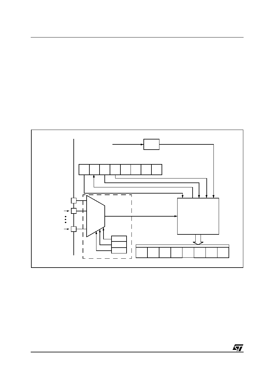
ST6200C/ST6201C/ST6203C
48/100
8.3 A/D CONVERTER (ADC)
8.3.1 Introduction
The on-chip Analog to Digital Converter (ADC) pe-
ripheral is a 8-bit, successive approximation con-
verter. This peripheral has multiplexed analog in-
put channels (refer to device pin out description)
that allow the peripheral to convert the analog volt-
age levels from different sources.
The result of the conversion is stored in a 8-bit
Data Register. The A/D converter is controlled
through a Control Register.
8.3.2 Main Features
s
8-bit conversion
s
Multiplexed analog input channels
s
Linear successive approximation
s
Data register (DR) which contains the results
s
End of Conversion flag
s
On/Off bit (to reduce consumption)
s
Typical conversion time 70 µs (with an 8 MHz
crystal)
The block diagram is shown in
Figure 28
.
Figure 28. ADC Block Diagram
Note: ADC not present on some devices. See device summary on page 1.
OSC
AD
EAI EOC STA PDS
ADCR
AIN0
AIN1
ANALOG TO DIGITAL
CONVERTER
AINx
PORT
MUX
ADR2 ADR1
ADR3
ADR7 ADR6 ADR5 ADR4
ADR0
ADR
DIV 12
f
ADC
f
INT
DDRx
ORx
DRx
I/O PORT
OFF
CR3
AD
CR1
AD
CR0
1

ST6200C/ST6201C/ST6203C
49/100
A/D CONVERTER (Cont'd)
8.3.3 Functional Description
8.3.3.1 Analog Power Supply
The high and low level reference voltage pins are
internally connected to the V
DD
and V
SS
pins.
Conversion accuracy may therefore be impacted
by voltage drops and noise in the event of heavily
loaded or badly decoupled power supply lines.
8.3.3.2 Digital A/D Conversion Result
The conversion is monotonic, meaning that the re-
sult never decreases if the analog input does not
and never increases if the analog input does not.
If the input voltage (V
AIN
) is greater than or equal
to V
DDA
(high-level voltage reference) then the
conversion result in the DR register is FFh (full
scale) without overflow indication.
If input voltage (V
AIN
) is lower than or equal to
V
SSA
(low-level voltage reference) then the con-
version result in the DR register is 00h.
The A/D converter is linear and the digital result of
the conversion is stored in the ADR register. The
accuracy of the conversion is described in the par-
ametric section.
R
AIN
is the maximum recommended impedance
for an analog input signal. If the impedance is too
high, this will result in a loss of accuracy due to
leakage and sampling not being completed in the
allocated time. Refer to the electrical characteris-
tics chapter for more details.
With an oscillator clock frequency less than
1.2MHz, conversion accuracy is decreased.
8.3.3.3 Analog Input Selection
Selection of the input pin is done by configuring
the related I/O line as an analog input via the Data
Direction, Option and Data registers (refer to I/O
ports description for additional information).
Caution: Only one I/O line must be configured as
an analog input at any time. The user must avoid
any situation in which more than one I/O pin is se-
lected as an analog input simultaneously, because
they will be shorted internally.
8.3.3.4 Software Procedure
Refer to the Control register (ADCR) and Data reg-
ister (ADR) in
Section 8.3.7
for the bit definitions.
Analog Input Configuration
The analog input must be configured through the
Port Control registers (DDRx, ORx and DRx). Re-
fer to the I/O port chapter.
ADC Configuration
In the ADCR register:
≠ Reset the PDS bit to power on the ADC. This bit
must be set at least one instruction before the
beginning of the conversion to allow stabilisation
of the A/D converter.
≠ Set the EAI bit to enable the ADC interrupt if
needed.
ADC Conversion
In the ADCR register:
≠ Set the STA bit to start a conversion. This auto-
matically clears (resets to "0") the End Of Con-
version Bit (EOC).
When a conversion is complete
≠ The EOC bit is set by hardware to flag that con-
version is complete and that the data in the ADC
data conversion register is valid.
≠ An interrupt is generated if the EAI bit was set
Setting the STA bit will start a new count and will
clear the EOC bit (thus clearing the interrupt con-
dition)
Note:
Setting the STA bit must be done by a different in-
struction from the instruction that powers-on the
ADC (setting the PDS bit) in order to make sure
the voltage to be converted is present on the pin.
Each conversion has to be separately initiated by
writing to the STA bit.
The STA bit is continuously scanned so that, if the
user sets it to "1" while a previous conversion is in
progress, a new conversion is started before com-
pleting the previous one. The start bit (STA) is a
write only bit, any attempt to read it will show a log-
ical "0".
1
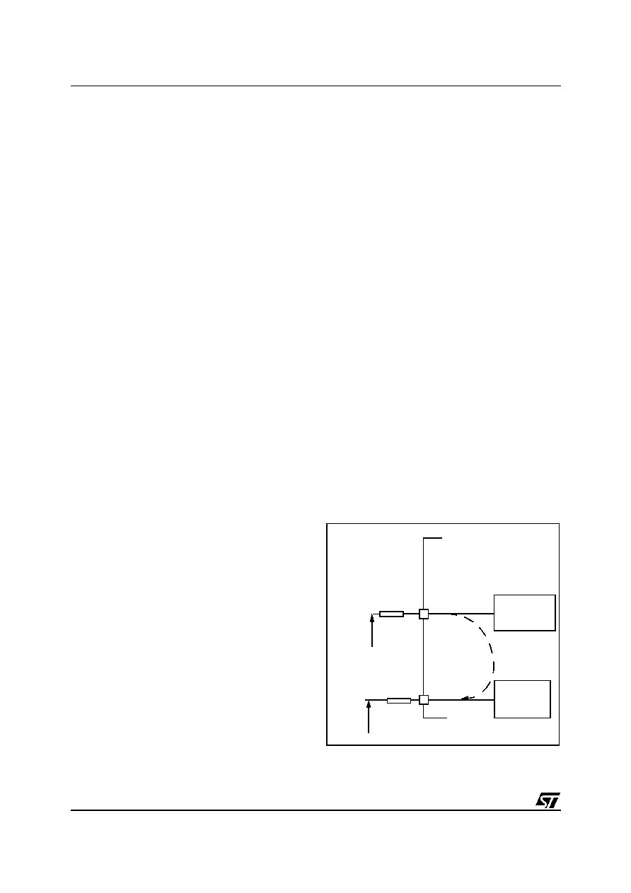
ST6200C/ST6201C/ST6203C
50/100
A/D CONVERTER (Cont'd)
8.3.4 Recommendations
The following six notes provide additional informa-
tion on using the A/D converter.
1.The A/D converter does not feature a sample
and hold circuit. The analog voltage to be meas-
ured should therefore be stable during the entire
conversion cycle. Voltage variation should not ex-
ceed ±1/2 LSB for optimum conversion accuracy.
A low pass filter may be used at the analog input
pins to reduce input voltage variation during con-
version.
2. When selected as an analog channel, the input
pin is internally connected to a capacitor C
ad
of
typically 9pF. For maximum accuracy, this capaci-
tor must be fully charged at the beginning of con-
version. In the worst case, conversion starts one
instruction (6.5 µs) after the channel has been se-
lected. The impedance of the analog voltage
source (ASI) in worst case conditions, is calculat-
ed using the following formula:
6.5µs = 9 x C
ad
x ASI
(capacitor charged to over 99.9%), i.e. 30 k
in-
cluding a 50% guardband.
The ASI can be higher if C
ad
has been charged for
a longer period by adding instructions before the
start of conversion (adding more than 26 CPU cy-
cles is pointless).
3. Since the ADC is on the same chip as the micro-
processor, the user should not switch heavily load-
ed output signals during conversion, if high preci-
sion is required. Such switching will affect the sup-
ply voltages used as analog references.
4. Conversion accuracy depends on the quality of
the power supplies (V
DD
and V
SS
). The user must
take special care to ensure a well regulated refer-
ence voltage is present on the V
DD
and V
SS
pins
(power supply voltage variations must be less than
0.1V/ms). This implies, in particular, that a suitable
decoupling capacitor is used at the V
DD
pin.
The converter resolution is given by:
The Input voltage (Ain) which is to be converted
must be constant for 1µs before conversion and
remain constant during conversion.
5. Conversion resolution can be improved if the
power supply voltage (V
DD
) to the microcontroller
is lowered.
6. In order to optimize the conversion resolution,
the user can configure the microcontroller in WAIT
mode, because this mode minimises noise distur-
bances and power supply variations due to output
switching. Nevertheless, the WAIT instruction
should be executed as soon as possible after the
beginning of the conversion, because execution of
the WAIT instruction may cause a small variation
of the V
DD
voltage. The negative effect of this var-
iation is minimized at the beginning of the conver-
sion when the converter is less sensitive, rather
than at the end of conversion, when the least sig-
nificant bits are determined.
The best configuration, from an accuracy stand-
point, is WAIT mode with the Timer stopped. In
this case only the ADC peripheral and the oscilla-
tor are then still working. The MCU must be woken
up from WAIT mode by the ADC interrupt at the
end of the conversion. The microcontroller can
also be woken up by the Timer interrupt, but this
means the Timer must be running and the result-
ing noise could affect conversion accuracy.
Caution: When an I/O pin is used as an analog in-
put, A/D conversion accuracy will be impaired if
negative current injections (V
INJ
< V
SS
) occur from
adjacent I/O pins with analog input capability. Re-
fer to
Figure 29
. To avoid this:
≠ Use another I/O port located further away from
the analog pin, preferably not multiplexed on the
A/D converter
≠ Increase the input resistance R
IN J
(to reduce the
current injections) and reduce R
ADC
(to preserve
conversion accuracy).
Figure 29. Leakage from Digital Inputs
V
DD
V
SS
≠
256
--------------------------------
PBy/AINy
PBx/AINx
R
ADC
Leakage Current
if V
INJ
< V
SS
A/D
I/O Port
(Digital I/O)
R
INJ
Converter
Digital
Input
Analog
Input
V
AIN
V
INJ
1
ST6200C/ST6201C/ST6203C
51/100
A/D CONVERTER (Cont'd)
8.3.5 Low Power Modes
Note: The A/D converter may be disabled by clear-
ing the PDS bit. This feature allows reduced power
consumption when no conversion is needed.
8.3.6 Interrupts
Note: The EOC bit is cleared only when a new
conversion is started (it cannot be cleared by writ-
ing 0). To avoid generating further EOC interrupt,
the EAI bit has to be cleared within the ADC inter-
rupt subroutine.
8.3.7 Register Description
A/D CONVERTER CONTROL REGISTER (AD-
CR)
Address: 0D1h - Read/Write (Bit 6 Read Only, Bit
5 Write Only)
Reset value: 0100 0000 (40h)
Bit 7 = EAI
Enable A/D Interrupt.
0: ADC interrupt disabled
1: ADC interrupt enabled
Bit 6 = EOC
End of conversion.
Read Only
When a conversion has been completed, this bit is
set by hardware and an interrupt request is gener-
ated if the EAI bit is set. The EOC bit is automati-
cally cleared when the STA bit is set. Data in the
data conversion register are valid only when this
bit is set to "1".
0: Conversion is not complete
1: Conversion can be read from the ADR register
Bit 5 = STA
: Start of Conversion. Write Only
.
0: No effect
1: Start conversion
Note: Setting this bit automatically clears the EOC
bit. If the bit is set again when a conversion is in
progress, the present conversion is stopped and a
new one will take place. This bit is write only, any
attempt to read it will show a logical zero.
Bit 4 = PDS
Power Down Selection.
0: A/D converter is switched off
1: A/D converter is switched on
Bit 3 = ADCR3 Reserved, must be cleared.
Bit 2 = OSCOFF
Main Oscillator off.
0: Main Oscillator enabled
1: Main Oscillator disabled
Note: This bit does not apply to the ADC peripher-
al but to the main clock system. Refer to the Clock
System section.
Bits 1:0 = ADCR[1:0] Reserved, must be cleared.
A/D CONVERTER DATA REGISTER (ADR)
Address: 0D0h - Read only
Reset value: xxxx xxxx (xxh)
Bits 7:0 = ADR[7:0]
: 8 Bit A/D Conversion Result.
Table 14. ADC Register Map and Reset Values
Mode Description
WAIT
No effect on A/D Converter. ADC interrupts
cause the device to exit from Wait mode.
STOP
A/D Converter disabled.
Interrupt Event
Event
Flag
Enable
Bit
Exit
from
Wait
Exit
from
Stop
End of Conver-
sion
EOC
EAI
Yes
No
7
0
EAI
EOC
STA
PDS
ADCR
3
OSC
OFF
ADCR
1
ADCR
0
7
0
ADR7
ADR6
ADR5
ADR4
ADR3
ADR2
ADR1
ADR0
Address
(Hex.)
Register
Label
7
6
5
4
3
2
1
0
0D0h
ADR
Reset Value
ADR7
0
ADR6
0
ADR5
0
ADR4
0
ADR3
0
ADR2
0
ADR1
0
ADR0
0
0D1h
ADCR
Reset Value
EAI
0
EOC
1
STA
0
PDS
0
ADCR3
0
OSCOFF
0
ADCR1
0
ADCR0
0
1

ST6200C/ST6201C/ST6203C
52/100
9 INSTRUCTION SET
9.1 ST6 ARCHITECTURE
The ST6 architecture has been designed for max-
imum efficiency while keeping byte usage to a
minimum; in short, to provide byte-efficient pro-
gramming. The ST6 core has the ability to set or
clear any register or RAM location bit in Data
space using a single instruction. Furthermore, pro-
grams can branch to a selected address depend-
ing on the status of any bit in Data space.
9.2 ADDRESSING MODES
The ST6 has nine addressing modes, which are
described in the following paragraphs. Three dif-
ferent address spaces are available: Program
space, Data space, and Stack space. Program
space contains the instructions which are to be ex-
ecuted, plus the data for immediate mode instruc-
tions. Data space contains the Accumulator, the X,
Y, V and W registers, peripheral and Input/Output
registers, the RAM locations and Data ROM loca-
tions (for storage of tables and constants). Stack
space contains six 12-bit RAM cells used to stack
the return addresses for subroutines and inter-
rupts.
Immediate. In immediate addressing mode, the
operand of the instruction follows the opcode loca-
tion. As the operand is a ROM byte, the immediate
addressing mode is used to access constants
which do not change during program execution
(e.g., a constant used to initialize a loop counter).
Direct. In direct addressing mode, the address of
the byte which is processed by the instruction is
stored in the location which follows the opcode. Di-
rect addressing allows the user to directly address
the 256 bytes in Data Space memory with a single
two-byte instruction.
Short Direct. The core can address the four RAM
registers X, Y, V, W (locations 80h, 81h, 82h, 83h)
in short-direct addressing mode. In this case, the
instruction is only one byte and the selection of the
location to be processed is contained in the op-
code. Short direct addressing is a subset of direct
addressing mode. (Note that 80h and 81h are also
indirect registers).
Extended. In extended addressing mode, the 12-
bit address needed to define the instruction is ob-
tained by concatenating the four least significant
bits of the opcode with the byte following the op-
code. The instructions (JP, CALL) which use ex-
tended addressing mode are able to branch to any
address in the 4 Kbyte Program space.
Extended addressing mode instructions are two
bytes long.
Program Counter Relative. Relative addressing
mode is only used in conditional branch instruc-
tions. The instruction is used to perform a test and,
if the condition is true, a branch with a span of -15
to +16 locations next to the address of the relative
instruction. If the condition is not true, the instruc-
tion which follows the relative instruction is execut-
ed. Relative addressing mode instructions are one
byte long. The opcode is obtained by adding the
three most significant bits which characterize the
test condition, one bit which determines whether it
is a forward branch (when it is 0) or backward
branch (when it is 1) and the four least significant
bits which give the span of the branch (0h to Fh)
which must be added or subtracted from the ad-
dress of the relative instruction to obtain the
branch destination address.
Bit Direct. In bit direct addressing mode, the bit to
be set or cleared is part of the opcode, and the
byte following the opcode points to the address of
the byte in which the specified bit must be set or
cleared. Thus, any bit in the 256 locations of Data
space memory can be set or cleared.
Bit Test & Branch. Bit test and branch addressing
mode is a combination of direct addressing and
relative addressing. Bit test and branch instruc-
tions are three bytes long. The bit identification
and the test condition are included in the opcode
byte. The address of the byte to be tested is given
in the next byte. The third byte is the jump dis-
placement, which is in the range of -127 to +128.
This displacement can be determined using a la-
bel, which is converted by the assembler.
Indirect. In indirect addressing mode, the byte
processed by the register-indirect instruction is at
the address pointed to by the content of one of the
indirect registers, X or Y (80h, 81h). The indirect
register is selected by bit 4 of the opcode. Register
indirect instructions are one byte long.
Inherent. In inherent addressing mode, all the in-
formation necessary for executing the instruction
is contained in the opcode. These instructions are
one byte long.
1

ST6200C/ST6201C/ST6203C
53/100
9.3 INSTRUCTION SET
The ST6 offers a set of 40 basic instructions
which, when combined with nine addressing
modes, yield 244 usable opcodes. They can be di-
vided into six different types: load/store, arithme-
tic/logic, conditional branch, control instructions,
jump/call, and bit manipulation. The following par-
agraphs describe the different types.
All the instructions belonging to a given type are
presented in individual tables.
Load & Store. These instructions use one, two or
three bytes depending on the addressing mode.
For LOAD, one operand is the Accumulator and
the other operand is obtained from data memory
using one of the addressing modes.
For Load Immediate, one operand can be any of
the 256 data space bytes while the other is always
immediate data.
Table 15. Load & Store Instructions
Legend:
X, Y
Index Registers,
V, W Short Direct Registers
#
Immediate data (stored in ROM memory)
rr
Data space register
Affected
*
Not Affected
Instruction
Addressing Mode
Bytes
Cycles
Flags
Z
C
LD A, X
Short Direct
1
4
*
LD A, Y
Short Direct
1
4
*
LD A, V
Short Direct
1
4
*
LD A, W
Short Direct
1
4
*
LD X, A
Short Direct
1
4
*
LD Y, A
Short Direct
1
4
*
LD V, A
Short Direct
1
4
*
LD W, A
Short Direct
1
4
*
LD A, rr
Direct
2
4
*
LD rr, A
Direct
2
4
*
LD A, (X)
Indirect
1
4
*
LD A, (Y)
Indirect
1
4
*
LD (X), A
Indirect
1
4
*
LD (Y), A
Indirect
1
4
*
LDI A, #N
Immediate
2
4
*
LDI rr, #N
Immediate
3
4
*
*
1

ST6200C/ST6201C/ST6203C
54/100
INSTRUCTION SET (Cont'd)
Arithmetic and Logic. These instructions are
used to perform arithmetic calculations and logic
operations. In AND, ADD, CP, SUB instructions
one operand is always the accumulator while, de-
pending on the addressing mode, the other can be
either a data space memory location or an imme-
diate value. In CLR, DEC, INC instructions the op-
erand can be any of the 256 data space address-
es. In COM, RLC, SLA the operand is always the
accumulator.
Table 16. Arithmetic & Logic Instructions
Notes:
X,Y
Index Registers
V, W Short Direct Registers
Affected
# Immediate data (stored in ROM memory)
* Not Affected
rr Data space register
Instruction
Addressing Mode
Bytes
Cycles
Flags
Z
C
ADD A, (X)
Indirect
1
4
ADD A, (Y)
Indirect
1
4
ADD A, rr
Direct
2
4
ADDI A, #N
Immediate
2
4
AND A, (X)
Indirect
1
4
AND A, (Y)
Indirect
1
4
AND A, rr
Direct
2
4
ANDI A, #N
Immediate
2
4
CLR A
Short Direct
2
4
CLR r
Direct
3
4
*
*
COM A
Inherent
1
4
CP A, (X)
Indirect
1
4
CP A, (Y)
Indirect
1
4
CP A, rr
Direct
2
4
CPI A, #N
Immediate
2
4
DEC X
Short Direct
1
4
*
DEC Y
Short Direct
1
4
*
DEC V
Short Direct
1
4
*
DEC W
Short Direct
1
4
*
DEC A
Direct
2
4
*
DEC rr
Direct
2
4
*
DEC (X)
Indirect
1
4
*
DEC (Y)
Indirect
1
4
*
INC X
Short Direct
1
4
*
INC Y
Short Direct
1
4
*
INC V
Short Direct
1
4
*
INC W
Short Direct
1
4
*
INC A
Direct
2
4
*
INC rr
Direct
2
4
*
INC (X)
Indirect
1
4
*
INC (Y)
Indirect
1
4
*
RLC A
Inherent
1
4
SLA A
Inherent
2
4
SUB A, (X)
Indirect
1
4
SUB A, (Y)
Indirect
1
4
SUB A, rr
Direct
2
4
SUBI A, #N
Immediate
2
4
1

ST6200C/ST6201C/ST6203C
55/100
INSTRUCTION SET (Cont'd)
Conditional Branch. Branch instructions perform
a branch in the program when the selected condi-
tion is met.
Bit Manipulation Instructions. These instruc-
tions can handle any bit in Data space memory.
One group either sets or clears. The other group
(see Conditional Branch) performs the bit test
branch operations.
Control Instructions. Control instructions control
microcontroller operations during program execu-
tion.
Jump and Call. These two instructions are used
to perform long (12-bit) jumps or subroutine calls
to any location in the whole program space.
Table 17. Conditional Branch Instructions
Notes
:
b
3-bit address
rr
Data space register
e
5 bit signed displacement in the range -15 to +16
Affected. The tested bit is shifted into carry.
ee
8 bit signed displacement in the range -126 to +129
*
Not Affected
Table 18. Bit Manipulation Instructions
Notes:
b
3-bit address
*
Not Affected
rr
Data space register
Bit Manipulation Instructions should not be used on Port Data Registers and any registers with read only and/or write only bits (see I/O port
chapter)
Table 19. Control Instructions
Notes:
1.
This instruction is deactivated and a WAIT is automatically executed instead of a STOP if the watchdog function is selected.
Affected
*Not Affected
Table 20. Jump & Call Instructions
Notes:
abc 12-bit address
*
Not Affected
Instruction
Branch If
Bytes
Cycles
Flags
Z
C
JRC e
C = 1
1
2
*
*
JRNC e
C = 0
1
2
*
*
JRZ e
Z = 1
1
2
*
*
JRNZ e
Z = 0
1
2
*
*
JRR b, rr, ee
Bit = 0
3
5
*
JRS b, rr, ee
Bit = 1
3
5
*
Instruction
Addressing Mode
Bytes
Cycles
Flags
Z
C
SET b,rr
Bit Direct
2
4
*
*
RES b,rr
Bit Direct
2
4
*
*
Instruction
Addressing Mode
Bytes
Cycles
Flags
Z
C
NOP
Inherent
1
2
*
*
RET
Inherent
1
2
*
*
RETI
Inherent
1
2
STOP
(1)
Inherent
1
2
*
*
WAIT
Inherent
1
2
*
*
Instruction
Addressing Mode
Bytes
Cycles
Flags
Z
C
CALL abc
Extended
2
4
*
*
JP abc
Extended
2
4
*
*
1

ST6200C/ST6201C/ST6203C
56/100
Opcode Map Summary. The following table contains an opcode map for the instructions used by the ST6
LOW
0
0000
1
0001
2
0010
3
0011
4
0100
5
0101
6
0110
7
0111
LOW
HI
HI
0
0000
2
JRNZ 4
CALL 2
JRNC 5
JRR 2
JRZ
2
JRC 4
LD
0
0000
e
abc
e
b0,rr,ee
e NOP
#
e
a,(x)
1
pcr 2
ext 1
pcr 3
bt 1
pcr
1
prc 1
ind
1
0001
2
JRNZ 4
CALL 2
JRNC 5
JRS 2
JRZ 4
INC 2
JRC 4
LDI
1
0001
e
abc
e
b0,rr,ee
e
x
e
a,nn
1
pcr 2
ext 1
pcr 3
bt 1
pcr 1
sd 1
prc 2
imm
2
0010
2
JRNZ 4
CALL 2
JRNC 5
JRR 2
JRZ
2
JRC 4
CP
2
0010
e
abc
e
b4,rr,ee
e
#
e
a,(x)
1
pcr 2
ext 1
pcr 3
bt 1
pcr
1
prc 1
ind
3
0011
2
JRNZ 4
CALL 2
JRNC 5
JRS 2
JRZ 4
LD 2
JRC 4
CPI
3
0011
e
abc
e
b4,rr,ee
e
a,x
e
a,nn
1
pcr 2
ext 1
pcr 3
bt 1
pcr 1
sd 1
prc 2
imm
4
0100
2
JRNZ 4
CALL 2
JRNC 5
JRR 2
JRZ
2
JRC 4
ADD
4
0100
e
abc
e
b2,rr,ee
e
#
e
a,(x)
1
pcr 2
ext 1
pcr 3
bt 1
pcr
1
prc 1
ind
5
0101
2
JRNZ 4
CALL 2
JRNC 5
JRS 2
JRZ 4
INC 2
JRC 4
ADDI
5
0101
e
abc
e
b2,rr,ee
e
y
e
a,nn
1
pcr 2
ext 1
pcr 3
bt 1
pcr 1
sd 1
prc 2
imm
6
0110
2
JRNZ 4
CALL 2
JRNC 5
JRR 2
JRZ
2
JRC 4
INC
6
0110
e
abc
e
b6,rr,ee
e
#
e
(x)
1
pcr 2
ext 1
pcr 3
bt 1
pcr
1
prc 1
ind
7
0111
2
JRNZ 4
CALL 2
JRNC 5
JRS 2
JRZ 4
LD 2
JRC
7
0111
e
abc
e
b6,rr,ee
e
a,y
e
#
1
pcr 2
ext 1
pcr 3
bt 1
pcr 1
sd 1
prc
8
1000
2
JRNZ 4
CALL 2
JRNC 5
JRR 2
JRZ
2
JRC 4
LD
8
1000
e
abc
e
b1,rr,ee
e
#
e
(x),a
1
pcr 2
ext 1
pcr 3
bt 1
pcr
1
prc 1
ind
9
1001
2
JRNZ 4
CALL 2
JRNC 5
JRS 2
JRZ 4
INC 2
JRC
9
1001
e
abc
e
b1,rr,ee
e
v
e
#
1
pcr 2
ext 1
pcr 3
bt 1
pcr 1
sd 1
prc
A
1010
2
JRNZ 4
CALL 2
JRNC 5
JRR 2
JRZ
2
JRC 4
AND
A
1010
e
abc
e
b5,rr,ee
e
#
e
a,(x)
1
pcr 2
ext 1
pcr 3
bt 1
pcr
1
prc 1
ind
B
1011
2
JRNZ 4
CALL 2
JRNC 5
JRS 2
JRZ 4
LD 2
JRC 4
ANDI
B
1011
e
abc
e
b5,rr,ee
e
a,v
e
a,nn
1
pcr 2
ext 1
pcr 3
bt 1
pcr 1
sd 1
prc 2
imm
C
1100
2
JRNZ 4
CALL 2
JRNC 5
JRR 2
JRZ
2
JRC 4
SUB
C
1100
e
abc
e
b3,rr,ee
e
#
e
a,(x)
1
pcr 2
ext 1
pcr 3
bt 1
pcr
1
prc 1
ind
D
1101
2
JRNZ 4
CALL 2
JRNC 5
JRS 2
JRZ 4
INC 2
JRC 4
SUBI
D
1101
e
abc
e
b3,rr,ee
e
w
e
a,nn
1
pcr 2
ext 1
pcr 3
bt 1
pcr 1
sd 1
prc 2
imm
E
1110
2
JRNZ 4
CALL 2
JRNC 5
JRR 2
JRZ
2
JRC 4
DEC
E
1110
e
abc
e
b7,rr,ee
e
#
e
(x)
1
pcr 2
ext 1
pcr 3
bt 1
pcr
1
prc 1
ind
F
1111
2
JRNZ 4
CALL 2
JRNC 5
JRS 2
JRZ 4
LD 2
JRC
F
1111
e
abc
e
b7,rr,ee
e
a,w
e
#
1
pcr 2
ext 1
pcr 3
bt 1
pcr 1
sd 1
prc
Abbreviations for Addressing Modes: Legend:
dir
Direct
#
Indicates Illegal Instructions
sd
Short Direct
e
5-bit Displacement
imm
Immediate
b
3-bit Address
inh
Inherent
rr
1-byte Data space address
ext
Extended
nn
1-byte immediate data
b.d
Bit Direct
abc
12-bit address
bt
Bit
Test ee
8-bit
displacement
pcr
Program Counter Relative
ind Indirect
2
JRC
e
1
prc
Mnemonic
Addressing Mode
Bytes
Cycles
Operands
1

ST6200C/ST6201C/ST6203C
57/100
Opcode Map Summary (Continued)
LOW
8
1000
9
1001
A
1010
B
1011
C
1100
D
1101
E
1110
F
1111
LOW
HI
HI
0
0000
2
JRNZ 4
JP 2
JRNC 4
RES 2
JRZ 4
LDI 2
JRC 4
LD
0
0000
e
abc
e
b0,rr
e
rr,nn
e
a,(y)
1
pcr 2
ext 1
pcr 2
b.d 1
pcr 3
imm 1
prc 1
ind
1
0001
2
JRNZ 4
JP 2
JRNC 4
SET 2
JRZ 4
DEC 2
JRC 4
LD
1
0001
e
abc
e
b0,rr
e
x
e
a,rr
1
pcr 2
ext 1
pcr 2
b.d 1
pcr 1
sd 1
prc 2
dir
2
0010
2
JRNZ 4
JP 2
JRNC 4
RES 2
JRZ 4
COM 2
JRC 4
CP
2
0010
e
abc
e
b4,rr
e
a
e
a,(y)
1
pcr 2
ext 1
pcr 2
b.d 1
pcr
1
prc 1
ind
3
0011
2
JRNZ 4
JP 2
JRNC 4
SET 2
JRZ 4
LD 2
JRC 4
CP
3
0011
e
abc
e
b4,rr
e
x,a
e
a,rr
1
pcr 2
ext 1
pcr 2
b.d 1
pcr 1
sd 1
prc 2
dir
4
0100
2
JRNZ 4
JP 2
JRNC 4
RES 2
JRZ 2
RETI 2
JRC 4
ADD
4
0100
e
abc
e
b2,rr
e
e
a,(y)
1
pcr 2
ext 1
pcr 2
b.d 1
pcr 1
inh 1
prc 1
ind
5
0101
2
JRNZ 4
JP 2
JRNC 4
SET 2
JRZ 4
DEC 2
JRC 4
ADD
5
0101
e
abc
e
b2,rr
e
y
e
a,rr
1
pcr 2
ext 1
pcr 2
b.d 1
pcr 1
sd 1
prc 2
dir
6
0110
2
JRNZ 4
JP 2
JRNC 4
RES 2
JRZ 2
STOP 2
JRC 4
INC
6
0110
e
abc
e
b6,rr
e
e
(y)
1
pcr 2
ext 1
pcr 2
b.d 1
pcr 1
inh 1
prc 1
ind
7
0111
2
JRNZ 4
JP 2
JRNC 4
SET 2
JRZ 4
LD 2
JRC 4
INC
7
0111
e
abc
e
b6,rr
e
y,a
e
rr
1
pcr 2
ext 1
pcr 2
b.d 1
pcr 1
sd 1
prc 2
dir
8
1000
2
JRNZ 4
JP 2
JRNC 4
RES 2
JRZ
2
JRC 4
LD
8
1000
e
abc
e
b1,rr
e
#
e
(y),a
1
pcr 2
ext 1
pcr 2
b.d 1
pcr
1
prc 1
ind
9
1001
2
JRNZ 4
JP 2
JRNC 4
SET 2
JRZ 4
DEC 2
JRC 4
LD
9
1001
e
abc
e
b1,rr
e
v
e
rr,a
1
pcr 2
ext 1
pcr 2
b.d 1
pcr 1
sd 1
prc 2
dir
A
1010
2
JRNZ 4
JP 2
JRNC 4
RES 2
JRZ 4
RCL 2
JRC 4
AND
A
1010
e
abc
e
b5,rr
e
a
e
a,(y)
1
pcr 2
ext 1
pcr 2
b.d 1
pcr 1
inh 1
prc 1
ind
B
1011
2
JRNZ 4
JP 2
JRNC 4
SET 2
JRZ 4
LD 2
JRC 4
AND
B
1011
e
abc
e
b5,rr
e
v,a
e
a,rr
1
pcr 2
ext 1
pcr 2
b.d 1
pcr 1
sd 1
prc 2
dir
C
1100
2
JRNZ 4
JP 2
JRNC 4
RES 2
JRZ 2
RET 2
JRC 4
SUB
C
1100
e
abc
e
b3,rr
e
e
a,(y)
1
pcr 2
ext 1
pcr 2
b.d 1
pcr 1
inh 1
prc 1
ind
D
1101
2
JRNZ 4
JP 2
JRNC 4
SET 2
JRZ 4
DEC 2
JRC 4
SUB
D
1101
e
abc
e
b3,rr
e
w
e
a,rr
1
pcr 2
ext 1
pcr 2
b.d 1
pcr 1
sd 1
prc 2
dir
E
1110
2
JRNZ 4
JP 2
JRNC 4
RES 2
JRZ 2
WAIT 2
JRC 4
DEC
E
1110
e
abc
e
b7,rr
e
e
(y)
1
pcr 2
ext 1
pcr 2
b.d 1
pcr 1
inh 1
prc 1
ind
F
1111
2
JRNZ 4
JP 2
JRNC 4
SET 2
JRZ 4
LD 2
JRC 4
DEC
F
1111
e
abc
e
b7,rr
e
w,a
e
rr
1
pcr 2
ext 1
pcr 2
b.d 1
pcr 1
sd 1
prc 2
dir
Abbreviations for Addressing Modes: Legend:
dir
Direct
#
Indicates Illegal Instructions
sd
Short Direct
e
5-bit Displacement
imm
Immediate
b
3-bit Address
inh
Inherent
rr
1-byte Data space address
ext
Extended
nn
1-byte immediate data
b.d
Bit Direct
abc
12-bit address
bt
Bit
Test ee
8-bit
Displacement
pcr
Program Counter Relative
ind Indirect
2
JRC
e
1
prc
Mnemonic
Addressing Mode
Bytes
Cycles
Operands
1
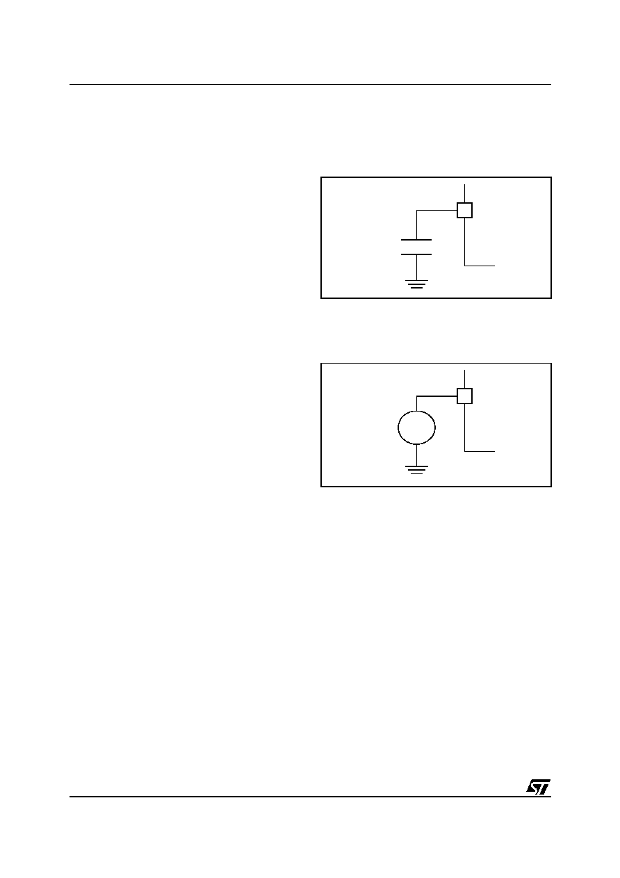
ST6200C/ST6201C/ST6203C
58/100
10 ELECTRICAL CHARACTERISTICS
10.1 PARAMETER CONDITIONS
Unless otherwise specified, all voltages are re-
ferred to V
SS
.
10.1.1 Minimum and Maximum Values
Unless otherwise specified the minimum and max-
imum values are guaranteed in the worst condi-
tions of ambient temperature, supply voltage and
frequencies by tests in production on 100% of the
devices with an ambient temperature at T
A
=25∞C
and T
A
=T
A
max (given by the selected temperature
range).
Data based on characterization results, design
simulation and/or technology characteristics are
indicated in the table footnotes and are not tested
in production. Based on characterization, the min-
imum and maximum values refer to sample tests
and represent the mean value plus or minus three
times the standard deviation (mean±3
).
10.1.2 Typical Values
Unless otherwise specified, typical data are based
on T
A
=25∞C, V
DD
=5V (for the 4.5V
V
DD
6.0V
voltage range) and V
DD
=3.3V (for the
3V
V
DD
3.6V voltage range). They are given only
as design guidelines and are not tested.
10.1.3 Typical Curves
Unless otherwise specified, all typical curves are
given only as design guidelines and are not tested.
10.1.4 Loading Capacitor
The loading conditions used for pin parameter
measurement is shown in
Figure 30
.
Figure 30. Pin Loading Conditions
10.1.5 Pin Input Voltage
The input voltage measurement on a pin of the de-
vice is described in
Figure 31
.
Figure 31. Pin Input Voltage
C
L
ST6 PIN
V
IN
ST6 PIN
1

ST6200C/ST6201C/ST6203C
59/100
10.2 ABSOLUTE MAXIMUM RATINGS
Stresses above those listed as "absolute maxi-
mum ratings" may cause permanent damage to
the device. This is a stress rating only and func-
tional operation of the device under these condi-
tions is not implied. Exposure to maximum rating
conditions for extended periods may affect device
reliability.
10.2.1 Voltage Characteristics
10.2.2 Current Characteristics
10.2.3 Thermal Characteristics
Notes:
1. Directly connecting the RESET and I/O pins to V
DD
or V
SS
could damage the device if an unintentional internal reset
is generated or an unexpected change of the I/O configuration occurs (for example, due to a corrupted program coun-
ter). To guarantee safe operation, this connection has to be done through a pull-up or pull-down resistor (typical: 4.7k
for RESET, 10k
for I/Os). Unused I/O pins must be tied in the same way to V
DD
or V
SS
according to their reset con-
figuration.
2. When the current limitation is not possible, the V
IN
absolute maximum rating must be respected, otherwise refer to
I
INJ(PIN)
specification. A positive injection is induced by V
IN
>V
DD
while a negative injection is induced by V
IN
<V
SS
.
3. Power (V
DD
) and ground (V
SS
) lines must always be connected to the external supply.
4. Negative injection disturbs the analog performance of the device. In particular, it induces leakage currents throughout
the device including the analog inputs. To avoid undesirable effects on the analog functions, care must be taken:
- Analog input pins must have a negative injection less than 1mA (assuming that the impedance of the analog voltage
is lower than the specified limits).
- Pure digital pins must have a negative injection less than 1mA. In addition, it is recommended to inject the current as
far as possible from the analog input pins.
Symbol
Ratings
Maximum value
Unit
V
DD
- V
SS
Supply voltage
7
V
V
IN
Input voltage on any pin
1) & 2)
V
SS
-0.3 to V
DD
+0.3
V
OUT
Output voltage on any pin
1) & 2)
V
SS
-0.3 to V
DD
+0.3
V
ESD(HBM)
Electro-static discharge voltage (Human Body Model)
3500
Symbol
Ratings
Maximum value
Unit
I
VDD
Total current into V
DD
power lines (source)
3)
80
mA
I
VSS
Total current out of V
SS
ground lines (sink)
3)
100
I
IO
Output current sunk by any standard I/O and control pin
20
Output current sunk by any high sink I/O pin
40
Output current source by any I/Os and control pin
15
I
INJ(PIN)
2) & 4)
Injected current on RESET pin
±
5
Injected current on any other pin
±
5
Symbol
Ratings
Value
Unit
T
STG
Storage temperature range
-60 to +150
∞C
T
J
Maximum junction temperature
(
see THERMAL CHARACTERISTICS section
)
1
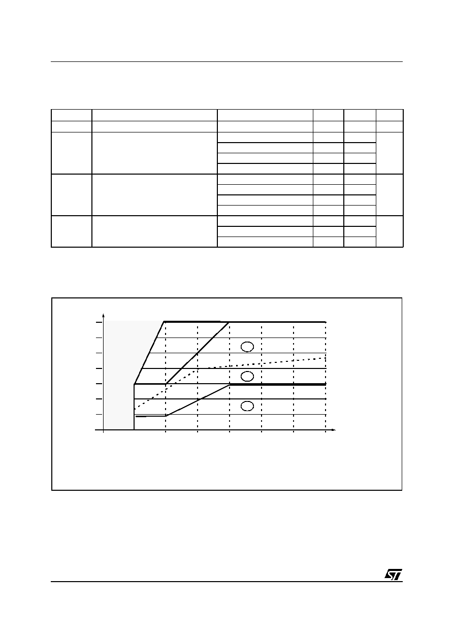
ST6200C/ST6201C/ST6203C
60/100
10.3 OPERATING CONDITIONS
10.3.1 General Operating Conditions
Notes:
1. An oscillator frequency above 1.2MHz is recommended for reliable A/D results.
2. Operating conditions with T
A
=-40 to +125∞C.
Figure 32. f
OSC
Maximum Operating Frequency Versus V
DD
Supply Voltage for OTP & ROM devices
Symbol
Parameter
Conditions
Min
Max
Unit
V
DD
Supply voltage
see
Figure 32
3.0
6
V
f
OSC
Oscillator frequency
V
DD
=3.0V, 1 & 6 Suffix
0
1)
4
MHz
V
DD
=3.0V, 3 Suffix
0
1)
4
V
DD
=3.6V, 1 & 6Suffix
0
1)
8
V
DD
=3.6V, 3 Suffix
0
1)
4
V
DD
Operating Supply Voltage
f
OSC
=4MHz, 1 & 6 Suffix
3.0
6.0
V
f
OSC
=4MHz, 3 Suffix
3.0
6.0
f
OSC
=8MHz, 1 & 6 Suffix
3.6
6.0
f
OSC
=8MHz, 3 Suffix
4.5
6.0
T
A
Ambient temperature range
1 Suffix Version
0
70
∞C
6 Suffix Version
-40
85
3 Suffix Version
-40
125
1
2.5
3.6
4
4.5
5
5.5
6
8
7
6
5
4
3
2
SUPPLY
3
f
OSG
f
OSG
Min
f
OSC
[MHz]
FU
N
C
TI
O
N
A
L
I
T
Y
NO
T
G
U
A
RA
N
T
E
E
D
IN
T
H
I
S
AR
EA
3
VOLTAGE (V
DD
)
2
1
1. In this area, operation is guaranteed at the quartz crystal frequency.
2. When the OSG is disabled, operation in this area is guaranteed at the crystal frequency. When the
3. When the OSG is disabled, operation in this area is guaranteed at the quartz crystal frequency. When
OSG is enabled, operation in this area is guaranteed at a frequency of at least f
OSG
Min.
the OSG is enabled, access to this area is prevented. The internal frequency is kept at f
OSG
.
1 & 6 suffix version
3 suffix version
1
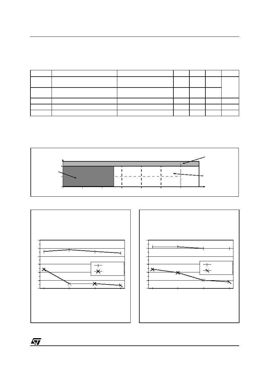
ST6200C/ST6201C/ST6203C
61/100
OPERATING CONDITIONS (Cont'd)
10.3.2 Operating Conditions with Low Voltage Detector (LVD)
Subject to general operating conditions for V
DD
, f
OSC
, and T
A
.
Notes:
1. LVD typical data are based on T
A
=25∞C. They are given only as design guidelines and are not tested.
2. The minimum V
DD
rise time rate is needed to insure a correct device power-on and LVD reset. Not tested in production.
3. Data based on characterization results, not tested in production.
Figure 33. LVD Threshold Versus V
DD
and f
OSC
3)
Figure 34. Typical LVD Thresholds Versus
Temperature for OTP devices
Figure 35. Typical LVD thresholds vs.
Temperature for ROM devices
Symbol
Parameter
Conditions
Min
Typ
1)
Max
Unit
V
IT+
Reset release threshold
(V
DD
rise)
3.9
4.1
4.3
V
V
IT-
Reset generation threshold
(V
DD
fall)
3.6
3.8
4
V
hys
LVD voltage threshold hysteresis
V
IT+
-V
IT-
50
300
700
mV
Vt
POR
V
DD
rise time rate
2)
mV/s
t
g(VDD)
Filtered glitch delay on V
DD
3)
Not detected by the LVD
30
ns
f
OSC
[MHz]
SUPPLY
8
4
0
2.5
3
3.5
4
4.5
5
5.5
FUNCTIONAL AREA
RESET
FUNCTIONALITY
NOT GUARANTEED
IN THIS AREA
V
IT-
3.6
DEVICE UNDER
IN THIS AREA
6
VOLTAGE [V]
-40∞C
25∞C
95∞C
125∞C
T [∞C]
3.6
3.8
4
4.2
Thresholds [V]
Vdd up
Vdd down
V
IT+
V
IT-
-40∞C
25∞C
95∞C
125∞C
T [∞C]
3.6
3.8
4
4.2
Thresholds [V]
Vdd up
Vdd down
V
IT+
V
IT-
1
ST6200C/ST6201C/ST6203C
62/100
10.4 SUPPLY CURRENT CHARACTERISTICS
The following current consumption specified for
the ST6 functional operating modes over tempera-
ture range does not take into account the clock
source current consumption. To get the total de-
vice consumption, the two current values must be
added (except for STOP mode for which the clock
is stopped).
10.4.1 RUN Modes
Notes:
1. Typical data are based on T
A
=25∞C, V
DD
=5V (4.5V
V
DD
6.0V range) and V
DD
=3.3V (3V
V
DD
3.6V range).
2. Data based on characterization results, tested in production at V
DD
max. and f
OSC
max.
3. CPU running with memory access, all I/O pins in input with pull-up mode (no load), all peripherals in reset state; clock
input (OSC
IN
) driven by external square wave, OSG and LVD disabled, option bytes not programmed.
Figure 36. Typical I
DD
in RUN vs. f
CPU
Figure 37. Typical I
DD
in RUN vs. Temperature
(V
DD
= 5V)
Symbol
Parameter
Conditions
Typ
1)
Max
2)
Unit
I
DD
Supply current in RUN mode
3)
(see
Figure 36
&
Figure 37
)
4.5
V
V
DD
6.
0V
f
OSC
=32kHz
f
OSC
=1MHz
f
OSC
=2MHz
f
OSC
=4MHz
f
OSC
=8MHz
0.5
1.3
1.6
2.2
3.3
0.7
1.7
2.4
3.3
4.8
mA
Supply current in RUN mode
3)
(see
Figure 36
&
Figure 37
)
3V
V
DD
3.6V
f
OSC
=32kHz
f
OSC
=1MHz
f
OSC
=2MHz
f
OSC
=4MHz
f
OSC
=8MHz
0.3
0.6
0.9
1.0
1.8
0.4
0.8
1.2
1.5
2.3
3
4
5
6
VDD [V]
0
1
2
3
4
5
IDD [mA]
8MHz
4MHz
2MHz
1MHz
32KHz
-40
25
95
125
T[∞C]
0
0.5
1
1.5
2
2.5
3
3.5
IDD [mA]
8MHz
4MHz
2MHz
1MHz
32KHz
1

ST6200C/ST6201C/ST6203C
63/100
SUPPLY CURRENT CHARACTERISTICS (Cont'd)
10.4.2 WAIT Modes
Notes:
1. Typical data are based on T
A
=25∞C, V
DD
=5V (4.5V
V
DD
6.0V range) and V
DD
=3.3V (3V
V
DD
3.6V range).
2. Data based on characterization results, tested in production at V
DD
max. and f
OSC
max.
3. All I/O pins in input with pull-up mode (no load), all peripherals in reset state; clock input (OSC
IN
) driven by external
square wave, OSG and LVD disabled.
Symbol
Parameter
Conditions
Typ
1)
Max
2)
Unit
I
DD
Supply current in WAIT mode
3)
Option bytes not programmed
(see
Figure 38
)
4.5V
V
DD
6.0V
OTP
devic
es
f
OSC
=32kHz
f
OSC
=1MHz
f
OSC
=2MHz
f
OSC
=4MHz
f
OSC
=8MHz
330
350
370
410
480
550
600
650
700
800
µA
Supply current in WAIT mode
3)
Option bytes programmed to 00H
(see
Figure 39
)
f
OSC
=32kHz
f
OSC
=1MHz
f
OSC
=2MHz
f
OSC
=4MHz
f
OSC
=8MHz
18
26
41
57
70
60
80
120
180
200
Supply current in WAIT mode
3)
(see
Figure 40
)
RO
M dev
ices
f
OSC
=32kHz
f
OSC
=1MHz
f
OSC
=2MHz
f
OSC
=4MHz
f
OSC
=8MHz
190
210
240
280
350
300
350
400
500
600
Supply current in WAIT mode
3)
Option bytes not programmed
(see
Figure 38
)
3V
V
DD
3.
6V
O
TP de
vices
f
OSC
=32kHz
f
OSC
=1MHz
f
OSC
=2MHz
f
OSC
=4MHz
f
OSC
=8MHz
80
90
100
120
150
120
140
150
200
250
Supply current in WAIT mode
3)
Option bytes programmed to 00H
(see
Figure 39
)
f
OSC
=32kHz
f
OSC
=1MHz
f
OSC
=2MHz
f
OSC
=4MHz
f
OSC
=8MHz
5
8
16
18
20
30
40
50
60
100
Supply current in WAIT mode
3)
Option bytes not programmed
(see
Figure 40
)
R
OM device
s
f
OSC
=32kHz
f
OSC
=1MHz
f
OSC
=2MHz
f
OSC
=4MHz
f
OSC
=8MHz
60
65
80
100
130
100
110
120
150
210
1
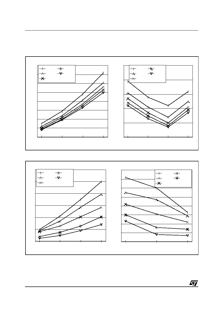
ST6200C/ST6201C/ST6203C
64/100
SUPPLY CURRENT CHARACTERISTICS (Cont'd)
Figure 38. Typical I
DD
in WAIT vs f
CPU
and Temperature for OTP devices with option bytes not
programmed
Figure 39. Typical I
DD
in WAIT vs f
CPU
and Temperature for OTP devices with option bytes
programmed to 00H
3
4
5
6
VDD [V]
0
100
200
300
400
500
600
700
800
IDD [µA]
8MHz
4MHz
2MHz
1M
32KHz
-40
25
95
125
T[∞C]
200
300
400
500
600
700
IDD [µA]
8MHz
4MHz
2MHz
1MHz
32KHz
3
4
5
6
VDD [V]
0
20
40
60
80
100
120
IDD [µA]
8MHz
4MHz
2MHz
1M
32KHz
-20
25
95
T[∞C]
10
20
30
40
50
60
70
80
90
IDD [µA]
8MHz
4MHz
2MHz
1MHz
32KHz
1
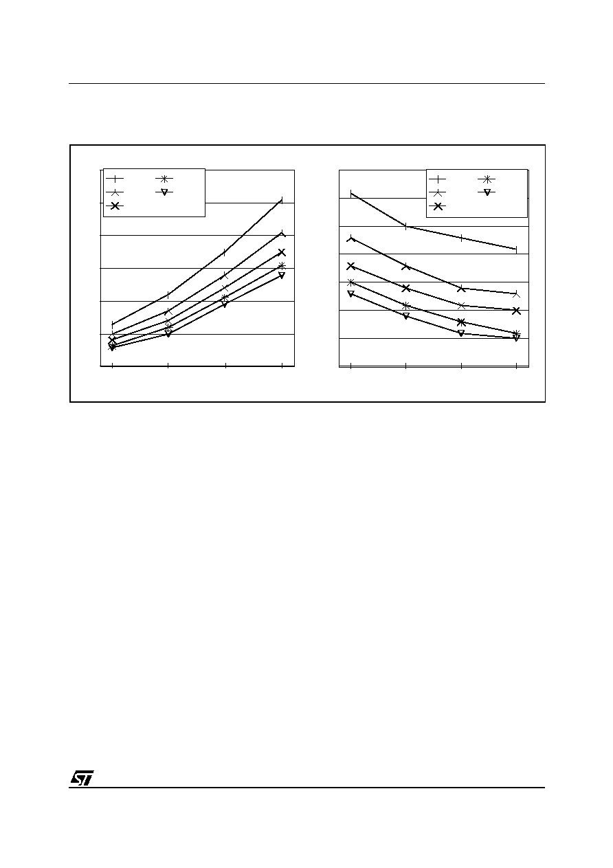
ST6200C/ST6201C/ST6203C
65/100
SUPPLY CURRENT CHARACTERISTICS (Cont'd)
Figure 40. Typical I
DD
in WAIT vs f
CPU
and Temperature for ROM devices
3
4
5
6
VDD [V]
0
100
200
300
400
500
600
IDD [µA]
8MHz
4MHz
2MHz
1M
32KHz
-20
25
95
125
T[∞C]
100
150
200
250
300
350
400
450
IDD [µA]
8MHz
4MHz
2MHz
1MHz
32KHz
1
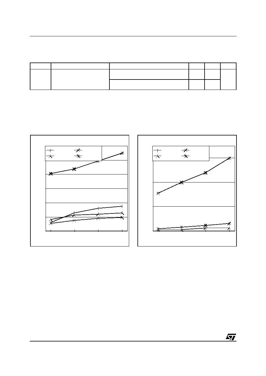
ST6200C/ST6201C/ST6203C
66/100
SUPPLY CURRENT CHARACTERISTICS (Cont'd)
10.4.3 STOP Mode
Notes:
1. Typical data are based on V
DD
=5.0V at T
A
=25∞C.
2. All I/O pins in input with pull-up mode (no load), all peripherals in reset state, OSG and LVD disabled, option bytes
programmed to 00H. Data based on characterization results, tested in production at V
DD
max. and f
CPU
max.
3. Maximum STOP consumption for -40∞C<Ta<90∞C
4. Maximum STOP consumption for -40∞C<Ta<125∞C
Figure 41. Typical I
DD
in STOP vs Temperature
for OTP devices
Figure 42. Typical I
DD
in STOP vs Temperature
for ROM devices
Symbol
Parameter
Conditions
Typ
1)
Max
Unit
I
DD
Supply current in STOP mode
2)
(see
Figure 41
&
Figure 42
)
OTP devices
0.3
10
3)
20
4)
µ
A
ROM devices
0.1
2
3)
20
4)
3
4
5
6
VDD [V]
0
200
400
600
800
1000
1200
IDD [nA]
Ta=-40∞C
Ta=25∞C
Ta=95∞C
Ta=125∞C
3
4
5
6
VDD [V]
0
500
1000
1500
IDD [nA]
Ta=-40∞C
Ta=25∞C
Ta=95∞C
Ta=125∞C
1
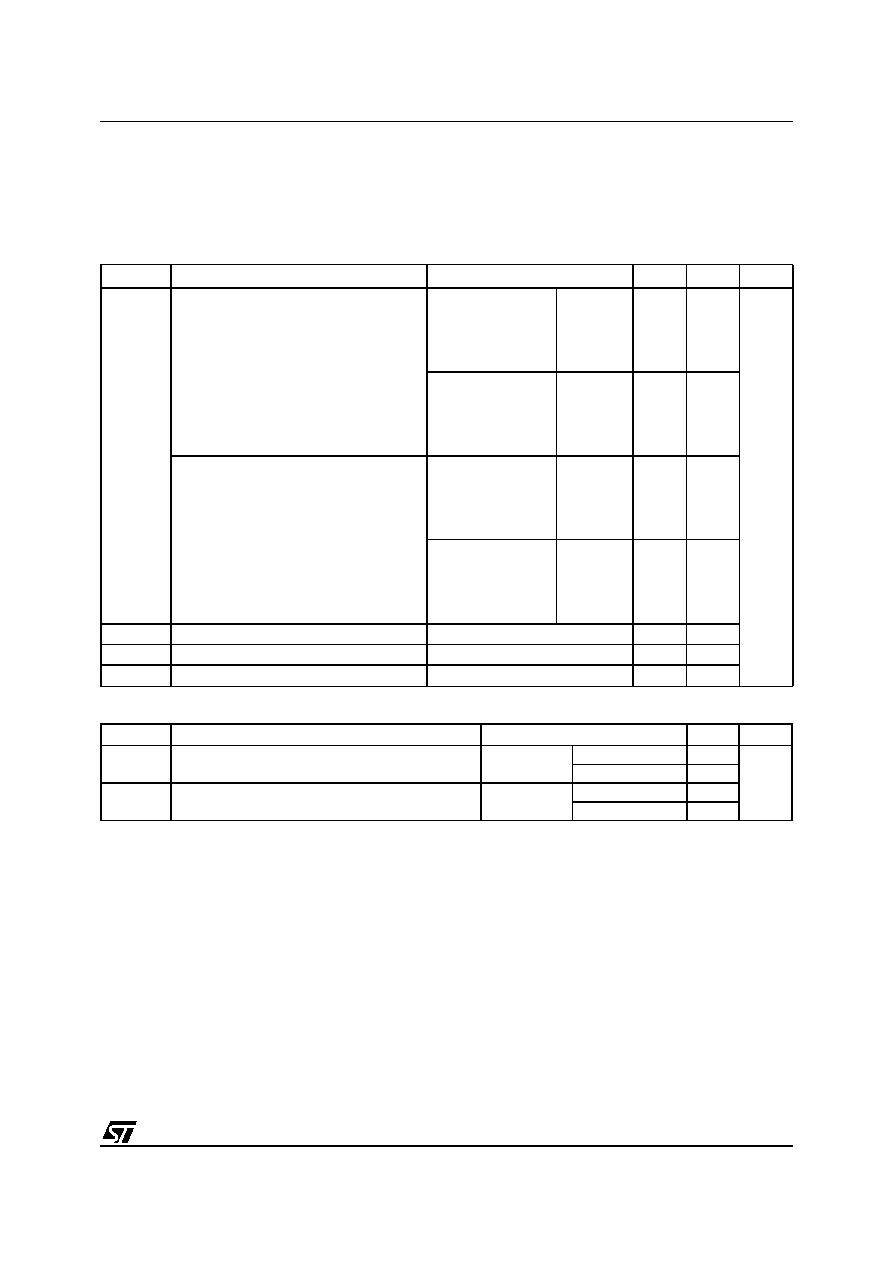
ST6200C/ST6201C/ST6203C
67/100
SUPPLY CURRENT CHARACTERISTICS (Cont'd)
10.4.4 Supply and Clock System
The previous current consumption specified for
the ST6 functional operating modes over tempera-
ture range does not take into account the clock
source current consumption. To get the total de-
vice consumption, the two current values must be
added (except for STOP mode).
10.4.5 On-Chip Peripherals
Notes:
1. Typical data are based on T
A
=25∞C.
2. Data based on characterization results, not tested in production.
3. Data based on a differential I
DD
measurement between reset configuration (OSG and LFAO disabled) and LFAO run-
ning (also includes the OSG stand alone consumption).
4. Data based on a differential I
DD
measurement between reset configuration with OSG disabled and OSG enabled.
5. Data based on a differential I
DD
measurement between reset configuration with LVD disabled and LVD enabled.
6. Data based on a differential I
DD
measurement between reset configuration (timer disabled) and timer running.
7. Data based on a differential I
DD
measurement between reset configuration and continuous A/D conversions.
Symbol
Parameter
Conditions
Typ
1)
Max
2)
Unit
I
DD(CK)
Supply current of RC oscillator
f
OSC
=32 kHz,
f
OSC
=1 MHz
f
OSC
=2 MHz
f
OSC
=4 MHz
f
OSC
=8 MHz
V
DD
=
5.0 V
230
260
340
480
µ
A
f
OSC
=32 kHz,
f
OSC
=1 MHz
f
OSC
=2 MHz
f
OSC
=4 MHz
f
OSC
=8 MHz
V
DD
=
3.3 V
80
110
180
320
Supply current of resonator oscillator
f
OSC
=32 kHz,
f
OSC
=1 MHz
f
OSC
=2 MHz
f
OSC
=4 MHz
f
OSC
=8MHz
V
DD
=
5.0 V
900
280
240
140
40
f
OSC
=32 kHz,
f
OSC
=1 MHz
f
OSC
=2 MHz
f
OSC
=4 MHz
f
OSC
=8 MHz
V
DD
=
3.3 V
120
70
50
20
10
I
DD(LFAO)
LFAO supply current
3)
V
DD
=
5.0 V
102
I
DD(OSG)
OSG supply current
4)
V
DD
=
5.0 V
40
I
DD(LVD)
LVD supply current
5)
V
DD
=
5.0 V
170
Symbol
Parameter
Conditions
Typ
1)
Unit
I
DD(TIM)
8-bit Timer supply current
6)
f
OSC
=8 MHz
V
DD
=
5.0 V
170
µA
V
DD
=
3.3 V
100
I
DD(ADC)
ADC supply current when converting
7)
f
OSC
=8 MHz
V
DD
=
5.0 V
80
V
DD
=
3.3 V
50
1

ST6200C/ST6201C/ST6203C
68/100
10.5 CLOCK AND TIMING CHARACTERISTICS
Subject to general operating conditions for V
DD
, f
OSC
, and T
A
.
10.5.1 General Timings
10.5.2 External Clock Source
Notes:
1. Data based on typical application software.
2. Time measured between interrupt event and interrupt vector fetch.
t
c(INST)
is the number of t
CPU
cycles needed to finish
the current instruction execution.
Figure 43. Typical Application with an External Clock Source
Symbol
Parameter
Conditions
Min
Typ
1)
Max
Unit
t
c(INST)
Instruction cycle time
2
4
5
t
CPU
f
CPU
=8 MHz
3.25
6.5
8.125
µ
s
t
v(IT)
Interrupt reaction time
2)
t
v(IT)
=
t
c(INST)
+ 6
6
11
t
CPU
f
CPU
=8 MHz
9.75
17.875
µ
s
Symbol
Parameter
Conditions
Min
Typ
Max
Unit
V
OSCINH
OSC
IN
input pin high level voltage
See
Figure 43
0.7xV
DD
V
DD
V
V
OSCINL
OSC
IN
input pin low level voltage
V
SS
0.3xV
DD
I
L
OSCx Input leakage current
V
SS
V
IN
V
DD
± 2
µ
A
OSC
IN
OSC
OUT
f
OSC
EXTERNAL
ST62XX
CLOCK SOURCE
V
OSCINL
V
OSCINH
I
L
90%
10%
Not connected
1
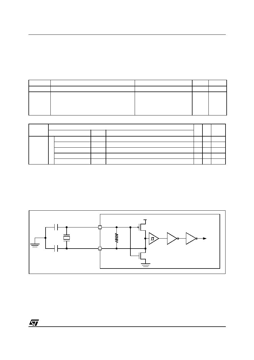
ST6200C/ST6201C/ST6203C
69/100
CLOCK AND TIMING CHARACTERISTICS (Cont'd)
10.5.3 Crystal and Ceramic Resonator Oscillators
The ST6 internal clock can be supplied with sever-
al different Crystal/Ceramic resonator oscillators.
Only parallel resonant crystals can be used. All the
information given in this paragraph are based on
characterization results with specified typical ex-
ternal components. Refer to the crystal/ceramic
resonator manufacturer for more details (frequen-
cy, package, accuracy...).
Notes:
1. Resonator characteristics given by the crystal/ceramic resonator manufacturer.
2. t
SU(OSC)
is the typical oscillator start-up time measured between V
DD
=2.8V and the fetch of the first instruction (with a
quick V
DD
ramp-up from 0 to 5V (<50
µ
s).
3. The oscillator selection can be optimized in terms of supply current using an high quality resonator with small R
S
value.
Refer to crystal/ceramic resonator manufacturer for more details.
Figure 44. Typical Application with a Crystal or Ceramic Resonator
Symbol
Parameter
Conditions
Typ
Unit
R
F
Feedback resistor
3
M
C
L1
C
L2
Recommended load capacitances versus equiva-
lent crystal or ceramic resonator frequency
f
OSC
=32 kHz,
f
OSC
=1 MHz
f
OSC
=2 MHz
f
OSC
=4 MHz
f
OSC
=8 MHz
120
47
33
33
22
pF
Oscillator
Typical Crystal or Ceramic Resonators
C
L1
[pF]
C
L2
[pF]
t
SU(osc)
[ms]
1)
Reference
Freq.
Characteristic
1)
Ce
ramic
MU
RATA
CSB455E
455KHz
f
OSC
=[±0.5KHz
tolerance
,±0.3%
Ta
,
±0.5%
aging
]
220 220
CSB1000J
1MHz
f
OSC
=[±0.5KHz
tolerance
,±0.3%
Ta
,
±0.5%
aging
]
100 100
CSTCC2.00MG0H6
2MHz
f
OSC
=[±0.5%
tolerance
,±0.5%
Ta
,
±0.3%
aging
]
47
47
CSTCC4.00MG0H6
4MHz
f
OSC
=[±0.5%
tolerance
,±0.3%
Ta
,
±0.3%
aging
]
47
47
CSTCC8.00MG
8MHz
f
OSC
=[±0.5%
tolerance
,±0.3%
Ta
,
±0.3%
aging
]
15
15
OSC
OUT
OSC
IN
C
L1
C
L2
R
F
ST62XX
RESONATOR
V
DD
F
OSC
1
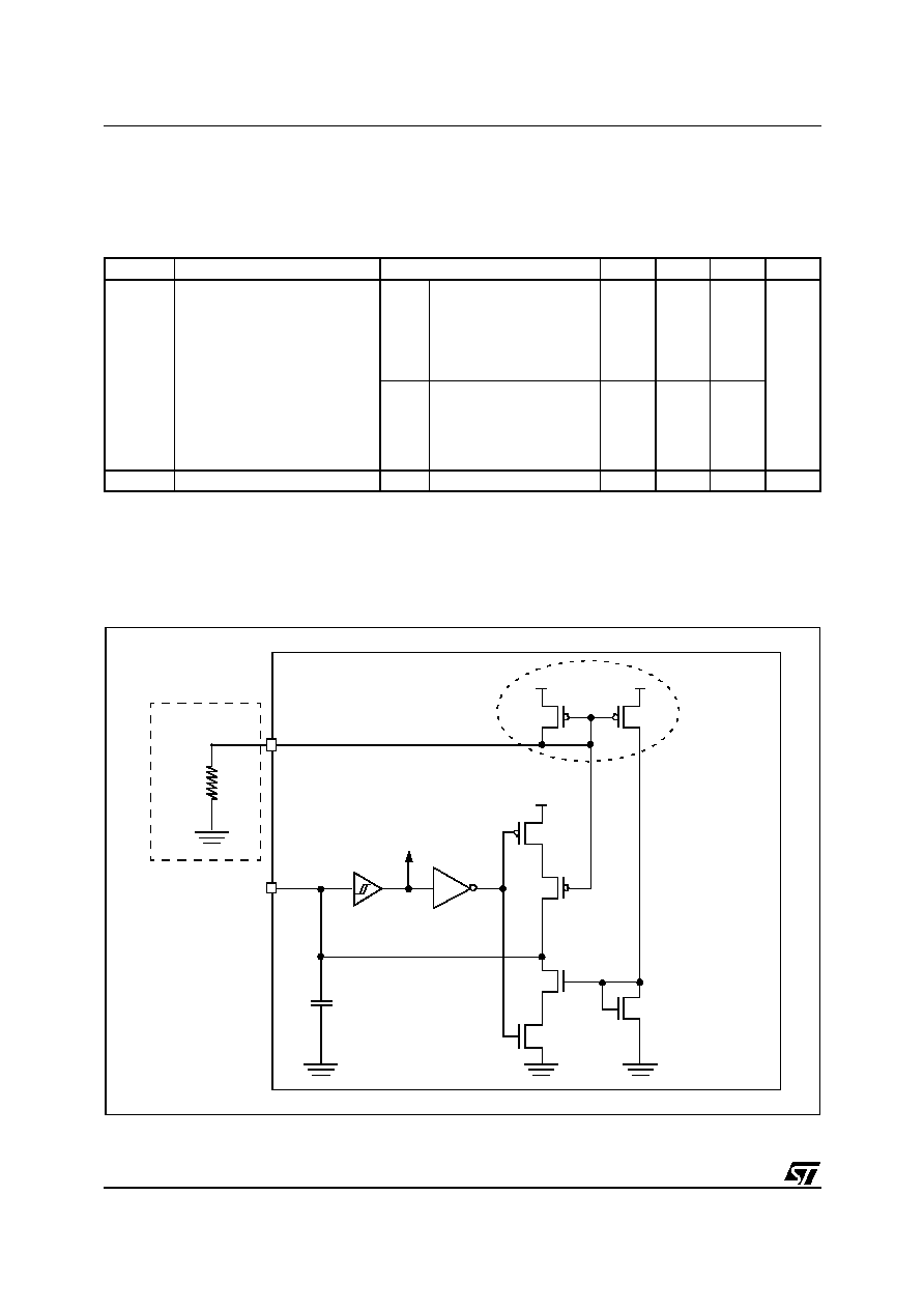
ST6200C/ST6201C/ST6203C
70/100
CLOCK AND TIMING CHARACTERISTICS (Cont'd)
10.5.4 RC Oscillator
The ST6 internal clock can be supplied with an external RC oscillator. Depending on the
R
NET
value, the
accuracy of the frequency is about 20%, so it may not be suitable for some applications.
Notes:
1. Data based on characterization results, not tested in production. These measurements were done with the OSCin pin
unconnected (only soldered on the PCB).
2. R
NET
must have a positive temperature coefficient (ppm/∞C), carbon resistors should therefore not be used.
Figure 45. Typical Application with RC Oscillator
Symbol
Parameter
Conditions
Min
Typ
Max
Unit
f
OSC
RC oscillator frequency
1)
4.5
V
V
DD
6.
0V
R
NET
=22 k
R
NET
=47 k
R
NET
=100 k
R
NET
=220 k
R
NET
=470 k
7.2
5.1
3.2
1.8
0.9
8.6
5.7
3.4
1.9
0.95
10
6.5
3.8
2
1.1
MHz
3V
V
DD
3.6V
R
NET
=22 k
R
NET
=47 k
R
NET
=100 k
R
NET
=220 k
R
NET
=470 k
3.7
2.8
1.8
1
0.5
4.3
3
1.9
1.1
0.55
4.9
3.3
2
1.2
0.6
R
NET
RC Oscillator external resistor
2)
see
Figure 46
&
Figure 47
22
870
k
OSC
IN
OSC
OUT
R
NET
EXTERNAL RC
C
EX
~9pF DISCHARGE
ST62XX
V
DD
V
DD
f
OSC
V
DD
NC
MIRROR
CURRENT
1
ST6200C/ST6201C/ST6203C
71/100
CLOCK AND TIMING CHARACTERISTICS (Cont'd)
Figure 46. Typical RC Oscillator frequency vs.
V
DD
Figure 47. Typical RC Oscillator frequency vs.
Temperature (V
DD
= 5V)
10.5.5 Oscillator Safeguard (OSG) and Low Frequency Auxiliary Oscillator (LFAO)
Figure 48. Typical LFAO Frequencies
Note:
1. Data based on characterization results.
3
4
5
6
VDD [V]
0
2
4
6
8
10
12
fosc [MHz]
Rnet=22KOhm
Rnet=47KOhm
Rnet=100KOhm
Rnet=220KOhm
Rnet=470KOhm
-40
25
95
125
Ta [∞C]
0
2
4
6
8
10
fosc [MHz]
Rnet=22KOhm
Rnet=47KOhm
Rnet=100KOhm
Rnet=220KOhm
Rnet=470KOhm
Symbol
Parameter
Conditions
Min
Typ
Max
Unit
f
LFAO
Low Frequency Auxiliary Oscillator
Frequency
1)
T
A
=
25∞ C, V
DD
=
5.0 V
200
350
800
kHz
T
A
=
25∞ C, V
DD
=
3.3 V
86
150
340
f
OSG
Internal Frequency with OSG ena-
bled
T
A
=
25∞ C, V
DD
=
4.5 V
4
MHz
T
A
=
25∞ C, V
DD
=
3.3 V
2
3
4
5
6
VDD [V]
0
100
200
300
400
500
600
fosc [kHz]
Ta=-40∞C
Ta=25∞C
Ta=125∞C
1
ST6200C/ST6201C/ST6203C
72/100
10.6 MEMORY CHARACTERISTICS
Subject to general operating conditions for V
DD
, f
OSC
, and T
A
unless otherwise specified.
10.6.1 RAM and Hardware Registers
10.6.2 EPROM Program Memory
Figure 49. EPROM Retention Time vs. Temperature
Notes:
1. Minimum V
DD
supply voltage without losing data stored in RAM (in STOP mode or under RESET) or in hardware reg-
isters (only in STOP mode). Guaranteed by construction, not tested in production.
2. Data based on reliability test results and monitored in production.
3. The data retention time increases when the T
A
decreases, see
Figure 49
.
Symbol
Parameter
Conditions
Min
Typ
Max
Unit
V
RM
Data retention
1)
0.7
V
Symbol
Parameter
Conditions
Min
Typ
Max
Unit
t
ret
Data retention
2)
T
A
=+55∞C
3)
10
years
-40
-30
-20
-10
0
10
20
30
40
50
60
70
80
90
100 110 120
Temperature [∞C]
0.1
1
10
100
1000
10000
100000
Retention time [Years]
1
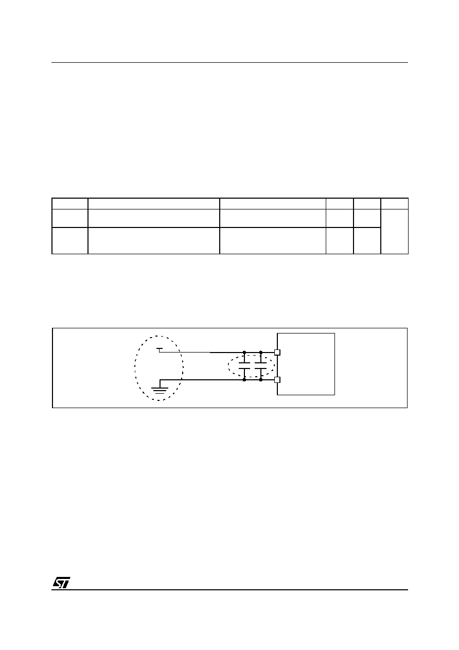
ST6200C/ST6201C/ST6203C
73/100
10.7 EMC CHARACTERISTICS
Susceptibility tests are performed on a sample ba-
sis during product characterization.
10.7.1 Functional EMS
(Electro Magnetic Susceptibility)
Based on a simple running application on the
product (toggling 2 LEDs through I/O ports), the
product is stressed by two electro magnetic events
until a failure occurs (indicated by the LEDs).
s
ESD: Electro-Static Discharge (positive and
negative) is applied on all pins of the device until
a functional disturbance occurs. This test
conforms with the IEC 1000-4-2 standard.
s
FTB: A Burst of Fast Transient voltage (positive
and negative) is applied to V
DD
and V
SS
through
a 100pF capacitor, until a functional disturbance
occurs. This test conforms with the IEC 1000-4-
4 standard.
A device reset allows normal operations to be re-
sumed.
Notes:
1. Data based on characterization results, not tested in production.
2. The suggested 10 µF and 0.1 µF decoupling capacitors on the power supply lines are proposed as a good price vs.
EMC performance tradeoff. They have to be put as close as possible to the device power supply pins. Other EMC rec-
ommendations are given in other sections (I/Os, RESET, OSCx pin characteristics).
Figure 50. EMC Recommended Star Network Power Supply Connection
2)
Symbol
Parameter
Conditions
Neg
1)
Pos
1)
Unit
V
FESD
Voltage limits to be applied on any I/O pin
to induce a functional disturbance
V
DD
=
5V, T
A
=
+25∞C, f
OSC
=
8MHz
conforms to IEC 1000-4-2
-2
2
kV
V
FFTB
Fast transient voltage burst limits to be ap-
plied through 100pF on V
DD
and V
DD
pins
to induce a functional disturbance
V
DD
=
5V, T
A
=
+25∞C, f
OSC
=
8MHz
conforms to IEC 1000-4-4
-2.5
3
V
DD
V
SS
0.1 µF
10 µF
V
DD
ST62XX
POWER
SUPPLY
SOURCE
ST6
DIGITAL NOISE
FILTERING
(close to the MCU)
1
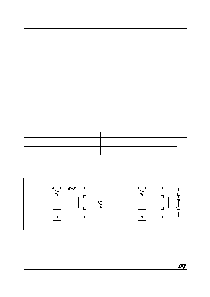
ST6200C/ST6201C/ST6203C
74/100
EMC CHARACTERISTICS (Cont'd)
10.7.2 Absolute Electrical Sensitivity
Based on three different tests (ESD, LU and DLU)
using specific measurement methods, the product
is stressed in order to determine its performance in
terms of electrical sensitivity. For more details, re-
fer to the AN1181 application note.
10.7.2.1 Electro-Static Discharge (ESD)
Electro-Static Discharges (3 positive then 3 nega-
tive pulses separated by 1 second) are applied to
the pins of each sample according to each pin
combination. The sample size depends of the
number of supply pins of the device (3 parts*(n+1)
supply pin). Two models are usually simulated:
Human Body Model and Machine Model. This test
conforms to the JESD22-A114A/A115A standard.
See
Figure 51
and the following test sequences.
Human Body Model Test Sequence
≠ C
L
is loaded through S1 by the HV pulse gener-
ator.
≠ S1 switches position from generator to R.
≠ A discharge from C
L
through R (body resistance)
to the ST6 occurs.
≠ S2 must be closed 10 to 100ms after the pulse
delivery period to ensure the ST6 is not left in
charge state. S2 must be opened at least 10ms
prior to the delivery of the next pulse.
Machine Model Test Sequence
≠ C
L
is loaded through S1 by the HV pulse gener-
ator.
≠ S1 switches position from generator to ST6.
≠ A discharge from C
L
to the ST6 occurs.
≠ S2 must be closed 10 to 100ms after the pulse
delivery period to ensure the ST6 is not left in
charge state. S2 must be opened at least 10ms
prior to the delivery of the next pulse.
≠ R (machine resistance), in series with S2, en-
sures a slow discharge of the ST6.
Absolute Maximum Ratings
Notes:
1. Data based on characterization results, not tested in production.
Figure 51. Typical Equivalent ESD Circuits
Symbol
Ratings
Conditions
Maximum value
1)
Unit
V
ESD(HBM)
Electro-static discharge voltage
(Human Body Model)
T
A
=
+25∞C
2000
V
V
ESD(MM)
Electro-static discharge voltage
(Machine Model)
T
A
=
+25∞C
200
ST6
S2
R=1500
S1
HIGH VOLTAGE
C
L
=
100pF
PULSE
GENERATOR
ST6
S2
HIGH VOLTAGE
C
L
=
200pF
PULSE
GENERATOR
R=
10k
~1
0M
S1
HUMAN BODY MODEL
MACHINE MODEL
1
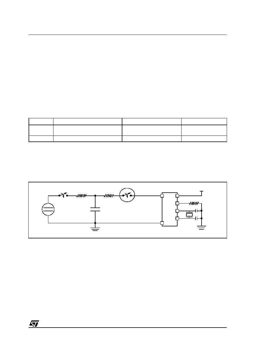
ST6200C/ST6201C/ST6203C
75/100
EMC CHARACTERISTICS (Cont'd)
10.7.2.2 Static and Dynamic Latch-Up
s
LU: 3 complementary static tests are required
on 10 parts to assess the latch-up performance.
A supply overvoltage (applied to each power
supply pin), a current injection (applied to each
input, output and configurable I/O pin) and a
power supply switch sequence are performed
on each sample. This test conforms to the EIA/
JESD 78 IC latch-up standard. For more details,
refer to the AN1181 application note.
s
DLU: Electro-Static Discharges (one positive
then one negative test) are applied to each pin
of 3 samples when the micro is running to
assess the latch-up performance in dynamic
mode. Power supplies are set to the typical
values, the oscillator is connected as near as
possible to the pins of the micro and the
component is put in reset mode. This test
conforms to the IEC1000-4-2 and SAEJ1752/3
standards and is described in
Figure 52
. For
more details, refer to the AN1181 application
note.
Electrical Sensitivities
Notes:
1. Class description: A Class is an STMicroelectronics internal specification. All its limits are higher than the JEDEC spec-
ifications, that means when a device belongs to Class A it exceeds the JEDEC standard. B Class strictly covers all the
JEDEC criteria (international standard).
2. Schaffner NSG435 with a pointed test finger.
Figure 52. Simplified Diagram of the ESD Generator for DLU
Symbol
Parameter
Conditions
Class
1)
LU
Static latch-up class
T
A
=
+25∞C
T
A
=
+85∞C
A
A
DLU
Dynamic latch-up class
V
DD
=
5V, f
OSC
=
4MHz, T
A
=
+25∞C
A
R
CH
=50M
R
D
=330
C
S
=
150pF
ESD
HV RELAY
DISCHARGE TIP
DISCHARGE
RETURN CONNECTION
GENERATOR
2)
ST6
V
DD
V
SS
1
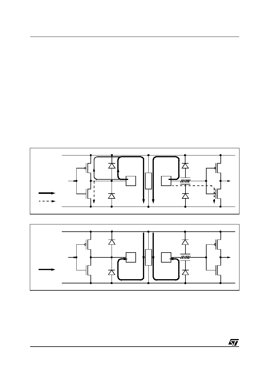
ST6200C/ST6201C/ST6203C
76/100
EMC CHARACTERISTICS (Cont'd)
10.7.3 ESD Pin Protection Strategy
To protect an integrated circuit against Electro-
Static Discharge the stress must be controlled to
prevent degradation or destruction of the circuit el-
ements. The stress generally affects the circuit el-
ements which are connected to the pads but can
also affect the internal devices when the supply
pads receive the stress. The elements to be pro-
tected must not receive excessive current, voltage
or heating within their structure.
An ESD network combines the different input and
output ESD protections. This network works, by al-
lowing safe discharge paths for the pins subjected
to ESD stress. Two critical ESD stress cases are
presented in
Figure 53
and
Figure 54
for standard
pins.
Standard Pin Protection
To protect the output structure the following ele-
ments are added:
≠ A diode to V
DD
(3a) and a diode from V
SS
(3b)
≠ A protection device between V
DD
and V
SS
(4)
To protect the input structure the following ele-
ments are added:
≠ A resistor in series with the pad (1)
≠ A diode to V
DD
(2a) and a diode from V
SS
(2b)
≠ A protection device between V
DD
and V
SS
(4)
Figure 53. Positive Stress on a Standard Pad vs. V
SS
Figure 54. Negative Stress on a Standard Pad vs. V
DD
IN
V
DD
V
SS
(1)
(2a)
(2b)
(4)
OUT
V
DD
V
SS
(3a)
(3b)
Main path
Path to avoid
IN
V
DD
V
SS
(1)
(2a)
(2b)
(4)
OUT
V
DD
V
SS
(3a)
(3b)
Main path
1

ST6200C/ST6201C/ST6203C
77/100
10.8 I/O PORT PIN CHARACTERISTICS
10.8.1 General Characteristics
Subject to general operating conditions for V
DD
, f
OSC
, and T
A
unless otherwise specified.
Figure 55. Typical R
PU
vs. V
DD
with V
IN
= V
SS
Notes:
1. Unless otherwise specified, typical data are based on T
A
=25∞C and V
DD
=5V.
2. Data based on characterization results, not tested in production.
3. Hysteresis voltage between Schmitt trigger switching levels. Based on characterization results, not tested.
4. The R
PU
pull-up equivalent resistor is based on a resistive transistor. This data is based on characterization results,
not tested in production.
5. Data based on characterization results, not tested in production.
6. To generate an external interrupt, a minimum pulse width has to be applied on an I/O port pin configured as an external
interrupt source.
Figure 56. Two typical Applications with unused I/O Pin
Symbol
Parameter
Conditions
Min
Typ
1)
Max
Unit
V
IL
Input low level voltage
2)
0.3xV
DD
V
V
IH
Input high level voltage
2)
0.7xV
DD
V
hys
Schmitt trigger voltage hysteresis
3)
V
DD
=5V
200
400
mV
V
DD
=3.3V
200
400
I
L
Input leakage current
V
SS
V
IN
V
DD
(no pull-up configured)
0.1
1
µ
A
R
PU
Weak pull-up equivalent resistor
4)
V
IN
=
V
SS
V
DD
=5V
40
110
350
k
V
DD
=3.3V
80
230
700
C
IN
I/O input pin capacitance
5
10
pF
C
OUT
I/O output pin capacitance
5
10
pF
t
f(IO)out
Output high to low level fall time
5)
C
L
=50pF
Between 10% and 90%
30
ns
t
r(IO)out
Output low to high level rise time
5)
35
t
w(IT)in
External interrupt pulse time
6)
1
t
CPU
3
4
5
6
VDD [V]
50
100
150
200
250
300
350
Rpu [Khom]
Ta=-40∞C
Ta=25∞C
Ta=95∞C
Ta=125∞C
10k
UNUSED I/O PORT
ST62XX
10k
UNUSED I/O PORT
ST62XX
V
DD
1

ST6200C/ST6201C/ST6203C
78/100
I/O PORT PIN CHARACTERISTICS (Cont'd)
10.8.2 Output Driving Current
Subject to general operating conditions for V
DD
, f
OSC
, and T
A
unless otherwise specified.
Notes:
1. The I
IO
current sunk must always respect the absolute maximum rating specified in
Section 10.2.2
and the sum of I
IO
(I/O ports and control pins) must not exceed I
VSS
.
2. The I
IO
current source must always respect the absolute maximum rating specified in
Section 10.2.2
and the sum of
I
IO
(I/O ports and control pins) must not exceed I
VDD
. True open drain I/O pins does not have V
OH
.
Figure 57. Typical V
OL
at V
DD
= 5V (standard)
Figure 58. Typical V
OL
at V
DD
= 5V (high-sink)
Symbol
Parameter
Conditions
Min
Max
Unit
V
OL
1)
Output low level voltage for a standard I/O pin
(see
Figure 57
and
Figure 60
)
V
DD
=5V
I
IO
=+10µA, T
A
125∞C
0.1
V
I
IO
=+3mA, T
A
125∞C
0.8
I
IO
=+5mA, T
A
85∞C
0.8
I
IO
=+10mA, T
A
85∞C
1.2
Output low level voltage for a high sink I/O pin
(see
Figure 58
and
Figure 61
)
I
IO
=+10µA, T
A
125∞C
0.1
I
IO
=+7mA, T
A
125∞C
0.8
I
IO
=+10mA, T
A
85∞C
0.8
I
IO
=+15mA, T
A
125∞C
1.3
I
IO
=+20mA, T
A
85∞C
1.3
I
IO
=+30mA, T
A
85∞C
2
V
OH
2)
Output high level voltage for an I/O pin
(see
Figure 59
and
Figure 62
)
I
IO
=-10
µ
A, T
A
125∞C
V
DD
-0.1
I
IO
=-3mA, T
A
125∞C
V
DD
-1.5
I
IO
=-5mA, T
A
85∞C
V
DD
-1.5
0
2
4
6
8
10
Iio [mA]
0
200
400
600
800
1000
Vol [mV] at Vdd=5V
Ta=-40∞C
Ta=25∞C
Ta=95∞C
Ta=125∞C
0
4
8
12
16
20
Iio [mA]
0
0.2
0.4
0.6
0.8
1
Vol [V] at Vdd=5V
Ta=-40∞C
Ta=25∞C
Ta=95∞C
Ta=125∞C
1
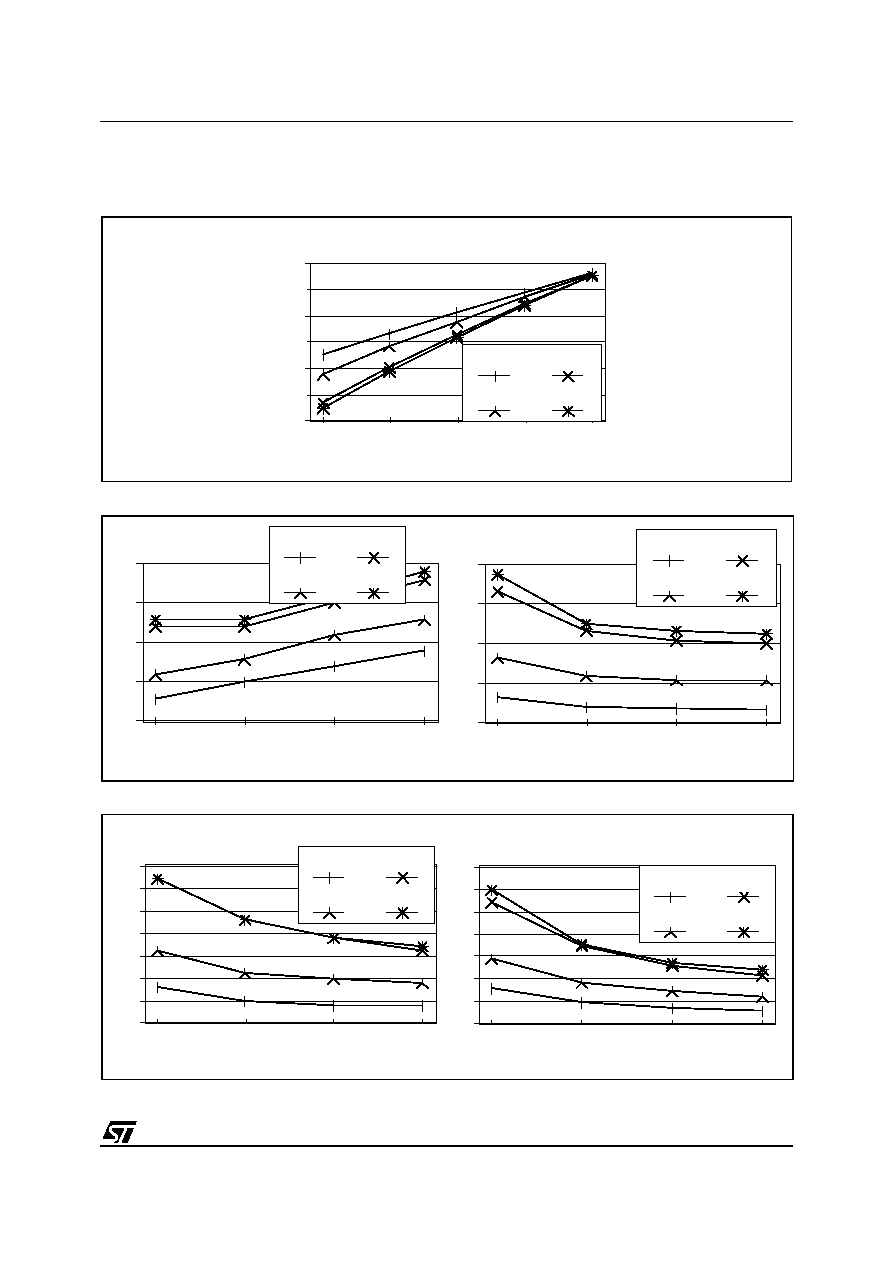
ST6200C/ST6201C/ST6203C
79/100
I/O PORT PIN CHARACTERISTICS (Cont'd)
Figure 59. Typical V
OH
at V
DD
= 5V
Figure 60. Typical V
OL
vs V
DD
(standard I/Os)
Figure 61. Typical V
OL
vs V
DD
(high-sink I/Os)
-8
-6
-4
-2
0
Iio [mA]
3.5
4
4.5
5
Voh [V] at Vdd=5V
Ta=-40∞C
Ta=25∞C
Ta=95∞C
Ta=125∞C
3
4
5
6
VDD [V]
150
200
250
300
350
Vol [mV] at Iio=2mA
Ta=-40∞C
Ta=25∞C
Ta=95∞C
Ta=125∞C
3
4
5
6
VDD [V]
300
400
500
600
700
Vol [mV] at Iio=5mA
Ta=-40∞C
Ta=25∞C
Ta=95∞C
Ta=125∞C
3
4
5
6
VDD [V]
0.2
0.25
0.3
0.35
0.4
0.45
0.5
0.55
Vol [V] at Iio=8mA
Ta=-40∞C
Ta=25∞C
Ta=95∞C
Ta=125∞C
3
4
5
6
VDD [V]
0.4
0.6
0.8
1
1.2
1.4
1.6
1.8
Vol [V] at Iio=20mA
Ta=-40∞C
Ta=25∞C
Ta=95∞C
Ta=125∞C
1

ST6200C/ST6201C/ST6203C
80/100
I/O PORT PIN CHARACTERISTICS (Cont'd)
Figure 62. Typical V
OH
vs V
DD
3
4
5
6
VDD [V]
2
3
4
5
6
Voh [V] at Iio=-2mA
Ta=-40∞C
Ta=25∞C
Ta=95∞C
Ta=125∞C
3
4
5
6
VDD [V]
1
2
3
4
5
6
Voh [V] at Iio=-5mA
Ta=-40∞C
Ta=25∞C
Ta=95∞C
Ta=125∞C
1
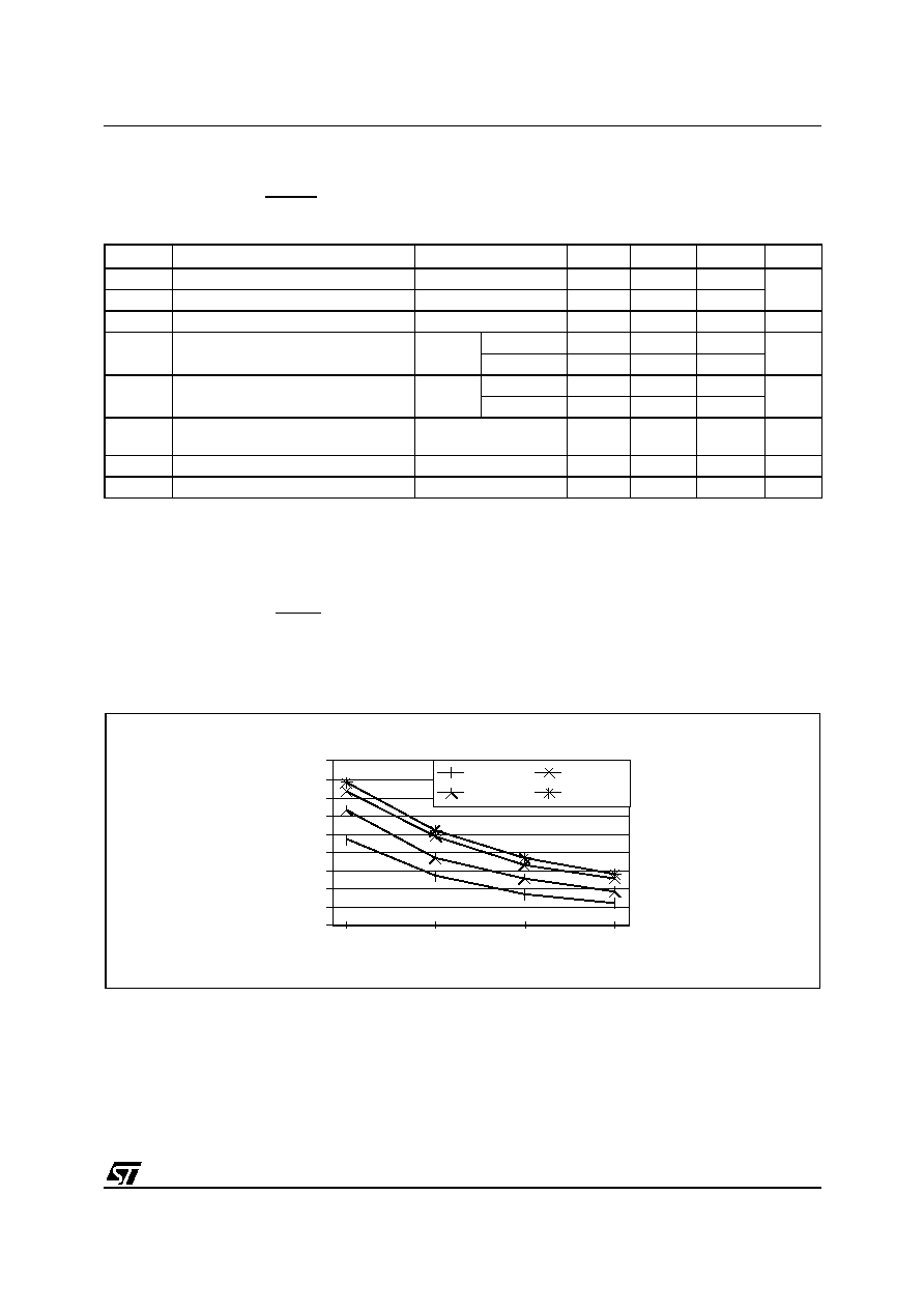
ST6200C/ST6201C/ST6203C
81/100
10.9 CONTROL PIN CHARACTERISTICS
10.9.1 Asynchronous RESET Pin
Subject to general operating conditions for V
DD
, f
OSC
, and T
A
unless otherwise specified.
Notes:
1. Unless otherwise specified, typical data are based on T
A
=25∞C and V
DD
=5V.
2. Data based on characterization results, not tested in production.
3. Hysteresis voltage between Schmitt trigger switching levels. Based on characterization results, not tested.
4. The R
ON
pull-up equivalent resistor is based on a resistive transistor. This data is based on characterization results,
not tested in production.
5. All short pulse applied on RESET pin with a duration below t
h(RSTL)in
can be ignored.
6. The reset network protects the device against parasitic resets, especially in a noisy environment.
7. The output of the external reset circuit must have an open-drain output to drive the ST6 reset pad. Otherwise the device
can be damaged when the ST6 generates an internal reset (LVD or watchdog).
Figure 63. Typical R
ON
vs V
DD
with V
IN
=V
SS
Symbol
Parameter
Conditions
Min
Typ
1)
Max
Unit
V
IL
Input low level voltage
2)
0.3xV
DD
V
V
IH
Input high level voltage
2)
0.7xV
DD
V
hys
Schmitt trigger voltage hysteresis
3)
200
400
mV
R
ON
Weak pull-up equivalent resistor
4)
V
IN
=
V
SS
V
DD
=5V
150
350
900
k
V
DD
=3.3V
300
730
1900
R
ESD
ESD resistor protection
V
IN
=
V
SS
V
DD
=5V
2.8
k
V
DD
=3.3V
t
w(RSTL)out
Generated reset pulse duration
External pin or
internal reset sources
t
CPU
µ
s
t
h(RSTL)in
External reset pulse hold time
5)
µ
s
t
g(RSTL)in
Filtered glitch duration
6)
ns
3
4
5
6
VDD [V]
100
200
300
400
500
600
700
800
900
1000
Ron [Kohm]
Ta=-40∞C
Ta=25∞C
Ta=95∞C
Ta=125∞C
1
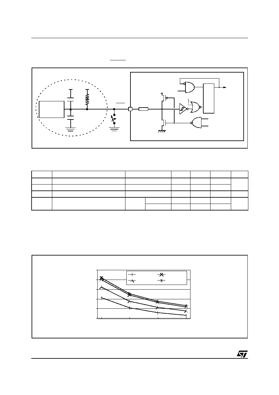
ST6200C/ST6201C/ST6203C
82/100
CONTROL PIN CHARACTERISTICS (Cont'd)
Figure 64. Typical Application with RESET pin
8)
10.9.2 NMI Pin
Subject to general operating conditions for V
DD
, f
OSC
, and T
A
unless otherwise specified.
Notes:
1. Unless otherwise specified, typical data are based on T
A
=25∞C and V
DD
=5V.
2. Data based on characterization results, not tested in production.
3. Hysteresis voltage between Schmitt trigger switching levels. Based on characterization results, not tested.
4. The R
pull-up
equivalent resistor is based on a resistive transistor. This data is based on characterization results, not
tested in production.
Figure 65. Typical R
pull-up
vs. V
DD
with V
IN
=V
SS
0.1
µ
F
V
DD
0.1
µ
F
V
DD
4.7k
EXTERNAL
RESET
CIRCUIT
7)
OP
TIO
N
AL
f
INT
CO
UNT
E
R
RESET
WATCHDOG RESET
LVD RESET
INTERNAL
RESET
R
ESD
1)
V
DD
R
PU
STOP MODE
20
48
ex
t
e
r
n
a
l
c
l
oc
k
c
y
c
l
es
Symbol
Parameter
Conditions
Min
Typ
1)
Max
Unit
V
IL
Input low level voltage
2)
0.3xV
DD
V
V
IH
Input high level voltage
2)
0.7xV
DD
V
hys
Schmitt trigger voltage hysteresis
3)
200
400
mV
R
pull-up
Weak pull-up equivalent resistor
4)
V
IN
=
V
SS
V
DD
=5V
40
100
350
k
V
DD
=3.3V
80
200
700
3
4
5
6
VDD [V]
50
100
150
200
250
300
Rpull-up [Kohm]
Ta=-40∞C
Ta=25∞C
Ta=95∞C
Ta=125∞C
1
ST6200C/ST6201C/ST6203C
83/100
CONTROL PIN CHARACTERISTICS (Cont'd)
10.10 TIMER PERIPHERAL CHARACTERISTICS
Subject to general operating conditions for V
DD
,
f
OSC
, and T
A
unless otherwise specified.
Refer to I/O port characteristics for more details on
the input/output alternate function characteristics
(TIMER).
10.10.1 Watchdog Timer
10.10.2 8-Bit Timer
Symbol
Parameter
Conditions
Min
Typ
Max
Unit
t
w(WDG)
Watchdog time-out duration
3,072
196,608
t
INT
f
CPU
=4MHz
0.768
49.152
ms
f
CPU
=8MHz
0.384
24.576
ms
Symbol
Parameter
Conditions
Min
Typ
Max
Unit
f
EXT
Timer external clock frequency
0
f
INT
/4
MHz
t
w
Pulse width at TIMER pin
VDD>4.5V
125
ns
VDD=3V
1
µs
1
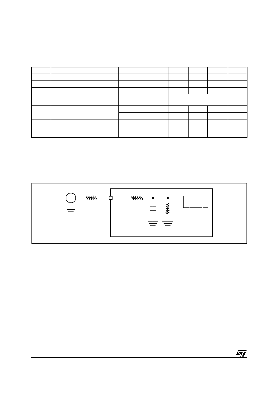
ST6200C/ST6201C/ST6203C
84/100
10.11 8-BIT ADC CHARACTERISTICS
Subject to general operating conditions for V
DD
, f
OSC
, and T
A
unless otherwise specified.
Notes:
1. Unless otherwise specified, typical data are based on T
A
=25∞C and V
DD
=5V.
2. The ADC refers to V
DD
and V
SS
.
3. Any added external serial resistor will downgrade the ADC accuracy (especially for resistance greater than 10k
). Data
based on characterization results, not tested in production.
4. As a stabilization time for the AD converter is required, the first conversion after the enable can be wrong.
Figure 66. Typical Application with ADC
Note: ADC not present on some devices. See device summary on page 1.
Symbol
Parameter
Conditions
Min
Typ
1)
Max
Unit
f
OSC
Clock frequency
1.2
f
OSC
MHz
V
AIN
Conversion range voltage
2)
V
SS
V
DD
V
R
AIN
External input resistor
10
3)
k
t
ADC
Total convertion time
f
OSC
=8MHz
f
OSC
=4MHz
70
140
µ
s
t
STAB
Stabilization time
4)
2
4
t
CPU
f
OSC
=8MHz
3.25
6.5
µs
AD
I
Analog input current during conver-
sion
1.0
µA
AC
IN
Analog input capacitance
2
5
pF
AINx
ST62XX
V
AIN
R
AIN
10pF
ADC
10M
r
150
1
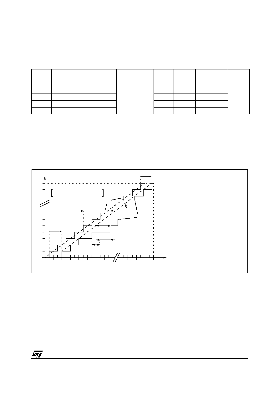
ST6200C/ST6201C/ST6203C
85/100
8-BIT ADC CHARACTERISTICS (Cont'd)
ADC Accuracy
Notes:
1. Negative injection disturbs the analog performance of the device. In particular, it induces leakage currents throughout
the device including the analog inputs. To avoid undesirable effects on the analog functions, care must be taken:
- Analog input pins must have a negative injection less than 1mA (assuming that the impedance of the analog voltage
is lower than the specified limits).
- Pure digital pins must have a negative injection less than 1mA. In addition, it is recommended to inject the current as
far as possible from the analog input pins.
2. Data based on characterization results over the whole temperature range, monitored in production.
Figure 67. ADC Accuracy Characteristics
Note: ADC not present on some devices. See device summary on page 1.
Symbol
Parameter
Conditions
Min
Typ.
Max
Unit
|E
T
|
Total unadjusted error
1)
V
DD
=5V
2)
f
OSC
=8MHz
1.2
±
2, fosc>1.2MHz
±
4, fosc>32KHz
LSB
E
O
Offset error
1)
0.72
E
G
Gain Error
1)
-0.31
|E
D
|
Differential linearity error
1)
0.54
|E
L
|
Integral linearity error
1)
E
O
E
G
1 LSB
IDEAL
1LSB
IDE AL
V
DDA
V
SSA
≠
256
-----------------------------------------
=
V
in
(LSB
IDEAL
)
(1) Example of an actual transfer curve
(2) The ideal transfer curve
(3) End point correlation line
E
T
=Total Unadjusted Error: maximum deviation
between the actual and the ideal transfer curves.
E
O
=Offset Error: deviation between the first actual
transition and the first ideal one.
E
G
=Gain Error: deviation between the last ideal
transition and the last actual one.
E
D
=Differential Linearity Error: maximum deviation
between actual steps and the ideal one.
E
L
=Integral Linearity Error: maximum deviation
between any actual transition and the end point
correlation line.
Digital Result ADCDR
255
254
253
5
4
3
2
1
0
7
6
1
2
3
4
5
6
7
253 254 255 256
(1)
(2)
E
T
E
D
E
L
(3)
V
DDA
V
SSA
1
ST6200C/ST6201C/ST6203C
86/100
11 GENERAL INFORMATION
11.1 PACKAGE MECHANICAL DATA
Figure 68. 16-Pin Plastic Dual In-Line Package, 300-mil Width
Figure 69. 16-Pin Plastic Small Outline Package, 300-mil Width
Dim.
mm
inches
Min
Typ
Max
Min
Typ
Max
A
5.33
0.210
A1
0.38
0.015
A2
2.92
3.30
4.95 0.115 0.130 0.195
b
0.36
0.46
0.56 0.014 0.018 0.022
b2
1.14
1.52
1.78 0.045 0.060 0.070
b3
0.76
0.99
1.14 0.030 0.039 0.045
c
0.20
0.25
0.36 0.008 0.010 0.014
D
18.67 19.18 19.69 0.735 0.755 0.775
D1
0.13
0.005
e
2.54
0.100
E
7.62
7.87
8.26 0.300 0.310 0.325
E1
6.10
6.35
7.11 0.240 0.250 0.280
L
2.92
3.30
3.81 0.115 0.130 0.150
eB
10.92
0.430
Number of Pins
N
16
c
E
E1
eB
L
A
A2
A1
e
b
b2
b3
D1
D
Dim.
mm
inches
Min
Typ
Max
Min
Typ
Max
A
2.35
2.65 0.093
0.104
A1
0.10
0.30 0.004
0.012
B
0.33
0.51 0.013
0.020
C
0.23
0.32 0.009
0.013
D
10.10
10.50 0.398
0.413
E
7.40
7.60 0.291
0.299
H
10.00
10.65 0.394
0.419
e
1.27
0.050
h
0.25
0.75 0.010
0.030
0∞
8∞
0∞
8∞
L
0.40
1.27 0.016
0.050
Number of Pins
N
16
H
E
C
h x 45◊
a
L
B
e
A1
A
D
1
ST6200C/ST6201C/ST6203C
87/100
PACKAGE MECHANICAL DATA (Cont'd)
Figure 70. 16-Pin Ceramic Side-Brazed Dual In-Line Package
Figure 71. 16-Pin Plastic Shrink Small Outline Package
Dim.
mm
inches
Min
Typ
Max
Min
Typ
Max
A
3.78
0.149
A1
0.38
0.015
B
0.36 0.46 0.56 0.014 0.018 0.022
B1
1.14 1.37 1.78 0.045 0.054 0.070
C
0.20 0.25 0.36 0.008 0.010 0.014
D
19.86 20.32 20.78 0.782 0.800 0.818
D1
17.78
0.700
E1
7.04 7.49 7.95 0.277 0.295 0.313
e
2.54
0.100
G
6.35 6.60 6.86 0.250 0.260 0.270
G1
9.47 9.73 9.98 0.373 0.383 0.393
G2
1.02
0.040
L
2.92 3.30 3.81 0.115 0.130 0.150
S
1.27
0.050
ÿ
4.22
0.166
Number of Pins
N
16
CDIP16W
Dim.
mm
inches
Min
Typ
Max
Min
Typ
Max
A
2.00
0.079
A1
0.05
0.002
A2
1.65
1.75
1.85 0.065 0.069 0.073
b
0.22
0.38 0.009
0.015
c
0.09
0.25 0.004
0.010
D
5.90
6.20
6.50 0.232 0.244 0.256
E
7.40
7.80
8.20 0.291 0.307 0.323
E1
5.00
5.30
5.60 0.197 0.209 0.220
e
0.65
0.026
0∞
4∞
8∞
0∞
4∞
8∞
L
0.55
0.75
0.95 0.022 0.030 0.037
Number of Pins
N
16
A2
A1
A
D
b
e
E1
E
L
h
c
1

ST6200C/ST6201C/ST6203C
88/100
11.2 THERMAL CHARACTERISTICS
Notes:
1. The power dissipation is obtained from the formula P
D
= P
INT
+ P
PORT
where P
INT
is the chip internal power (I
DD
xV
DD
)
and P
PORT
is the port power dissipation determined by the user.
2. The average chip-junction temperature can be obtained from the formula T
J
= T
A
+ P
D
x RthJA.
Symbol
Ratings
Value
Unit
R
thJA
Package thermal resistance (junction to ambient)
DIP16
SO16
SSOP16
90
90
125
∞C/W
P
D
Power dissipation
1)
500
mW
T
Jmax
Maximum junction temperature
2)
150
∞C
1
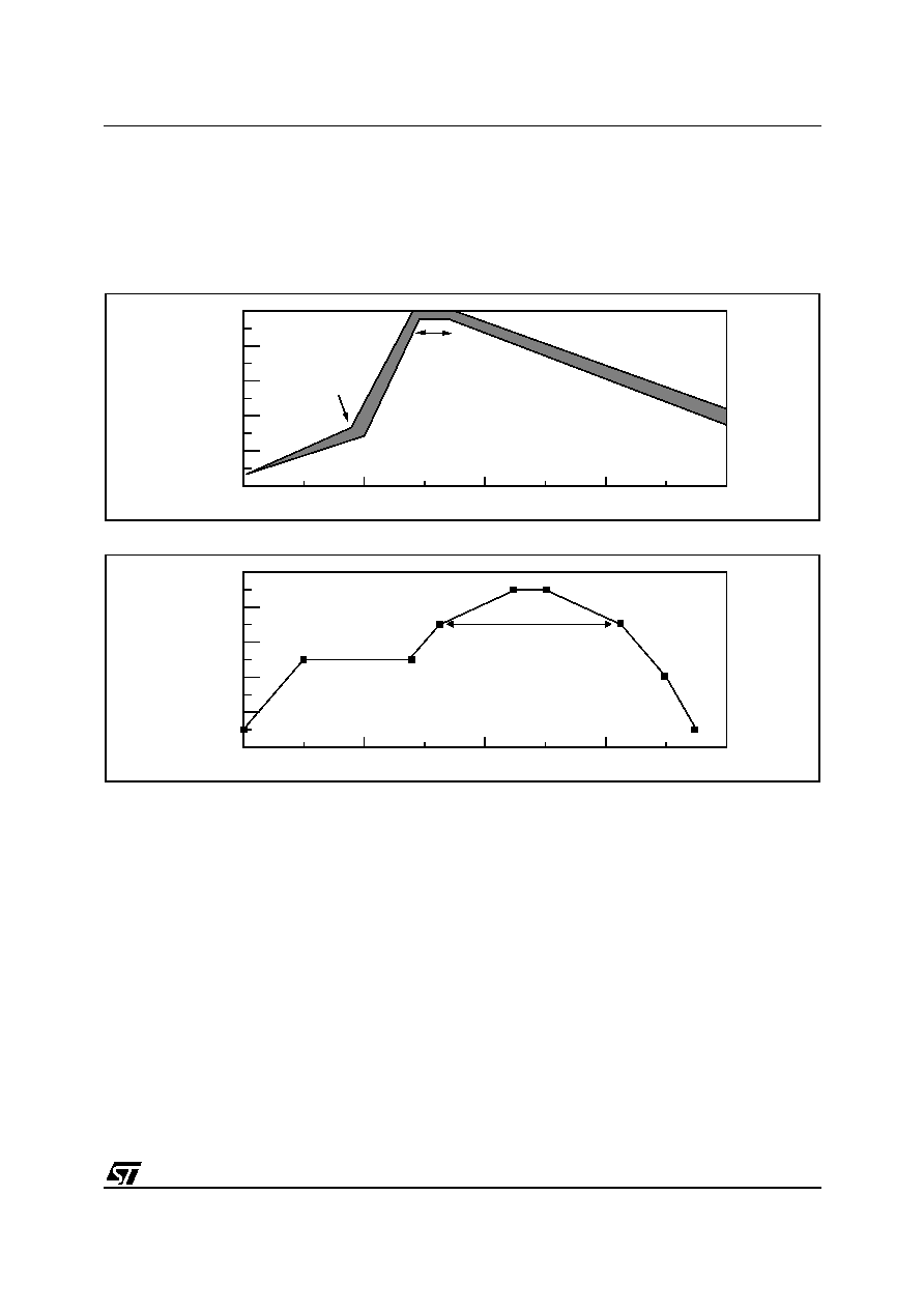
ST6200C/ST6201C/ST6203C
89/100
11.3 SOLDERING AND GLUEABILITY INFORMATION
Recommended soldering information given only
as design guidelines in
Figure 72
and
Figure 73
.
Recommended glue for SMD plastic packages:
s
Heraeus: PD945, PD955
s
Loctite: 3615, 3298
Figure 72. Recommended Wave Soldering Profile (with 37% Sn and 63% Pb)
Figure 73. Recommended Reflow Soldering Oven Profile (MID JEDEC)
250
200
150
100
50
0
40
80
120
160
Time [sec]
Temp. [∞C]
20
60
100
140
5 sec
COOLING PHASE
(ROOM TEMPERATURE)
PREHEATING
80∞C
PHASE
SOLDERING
PHASE
250
200
150
100
50
0
100
200
300
400
Time [sec]
Temp. [∞C]
ramp up
2∞C/sec for 50sec
90 sec at 125∞C
150 sec above 183∞C
ramp down natural
2∞C/sec max
Tmax=220+/-5∞C
for 25 sec
1
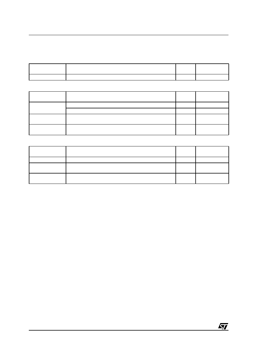
ST6200C/ST6201C/ST6203C
90/100
11.4 PACKAGE/SOCKET FOOTPRINT PROPOSAL
Table 21. Suggested List of DIP16 Socket Types
Table 22. Suggested List of SO16 Socket Types
Table 23. Suggested List of SSOP16 Socket Types
Package / Probe
Adaptor / Socket Reference
Same
Footprint
Socket Type
DIP16
TEXTOOL
216-33-40
X
Textool
Package / Probe
Adaptor / Socket Reference
Same
Footprint
Socket Type
SO16
ENPLAS
OTS-16-1.27-04
Open Top
YAMAICHI
IC51-347.KS-7704
Clamshell
EMU PROBE
Adapter from SO16 to DIP16 footprint
(delivered with emulator)
X
SMD to DIP
Programming
Adapter
Logical Systems
PA16SO1-08H-6
X
Open Top
Package / Probe
Adaptor / Socket Reference
Same
Footprint
Socket Type
SSOP16
ENPLAS
OTS-16-0.65-01
Open Top
EMU PROBE
Adapter from SSOP16 to DIP16 footprint
(sales type: ST626X-P/SSOP16)
X
SMD to DIP
Programming
Adapter
Logical Systems
PA16SS-OT-6
X
Open Top
1
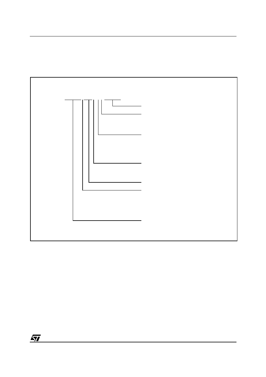
ST6200C/ST6201C/ST6203C
91/100
11.5 ORDERING INFORMATION
The following section deals with the procedure for
transfer of customer codes to STMicroelectronics
and also details the ST6 factory coded device
type.
Figure 74. ST6 Factory Coded Device Types
ROM code
Temperature code:
1: Standard 0 to +70 ∞C
3: Automotive -40 to +125 ∞C
6: Industrial -40 to +85 ∞C
Package type:
B: Plastic DIP
D: Ceramic DIP
M: Plastic SOP
N: Plastic SSOP
T: Plastic TQFP
Revision index:
B,C: Product Definition change
L: Low Voltage Device
ST6 Sub family
Version Code:
No char: ROM
E: EPROM
P: FASTROM
T: OTP
Family
ST62T03CB6/CCC
1
ST6200C/ST6201C/ST6203C
92/100
11.6 TRANSFER OF CUSTOMER CODE
Customer code is made up of the ROM contents
and the list of the selected FASTROM options.
The ROM contents are to be sent on diskette, or
by electronic means, with the hexadecimal file
generated by the development tool. All unused
bytes must be set to FFh.
The selected options are communicated to
STMicroelectronics using the correctly filled OP-
TION LIST appended. See
page 94
.
The STMicroelectronics Sales Organization will be
pleased to provide detailed information on con-
tractual points.
Listing Generation and Verification. When
STMicroelectronics receives the user's ROM con-
tents, a computer listing is generated from it. This
listing refers exactly to the ROM contents and op-
tions which will be used to produce the specified
MCU. The listing is then returned to the customer
who must thoroughly check, complete, sign and
return it to STMicroelectronics. The signed listing
forms a part of the contractual agreement for the
production of the specific customer MCU.
11.6.1 FASTROM version
The ST62P00C, P01C and P03C are the Factory
Advanced Service Technique ROM (FASTROM)
versions of ST62T00C, T01 and T03C OTP devic-
es.
They offer the same functionality as OTP devices,
but they do not have to be programmed by the
customer. The customer code must be sent to
STMicroelectronics in the same way as for ROM
devices. The FASTROM option list has the same
options as defined in the programmable option
byte of the OTP version. It also offers an identifier
option. If this option is enabled, each FASTROM
device is programmed with a unique 5-byte
number which is mapped at addresses 0F9Bh-
0F9Fh. The user must therefore leave these bytes
blanked.
The identification number is structured as follows:
with T0, T1, T2, T3 = time in seconds since 01/01/
1970 and Test ID = Tester Identifier.
0F9Bh
T0
0F9Ch
T1
0F9Dh
T2
0F9Eh
T3
0F9Fh
Test ID
1
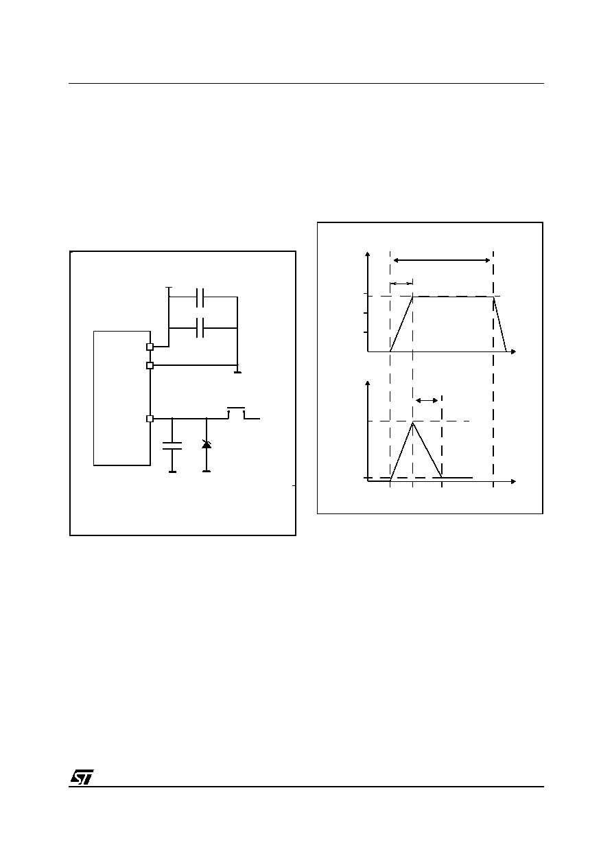
ST6200C/ST6201C/ST6203C
93/100
TRANSFER OF CUSTOMER CODE (Cont'd)
11.6.2 ROM VERSION
The ST6200C, 01C and 03C are mask pro-
grammed ROM version of ST62T00C, T01 and
T03C OTP devices.
They offer the same functionality as OTP devices,
selecting as ROM options the options defined in
the programmable option byte of the OTP version.
Figure 75. Programming Circuit
Note: ZPD15 is used for overvoltage protection
ROM Readout Protection. If the ROM READOUT
PROTECTION option is selected, a protection
fuse can be blown to prevent any access to the
program memory content.
In case the user wants to blow this fuse, high volt-
age must be applied on the V
PP
pin.
Figure 76. Programming wave form
VR02003
V
PP
5V
100nF
4.7µF
PROTECT
100nF
V
DD
V
SS
ZPD15
15V
14V
100 µs max
0.5s min
V
PP
15
14V typ
10
5
V
PP
400mA
4mA typ
VR02001
max
150 µs typ
t
1

ST6200C/ST6201C/ST6203C
94/100
TRANSFER OF CUSTOMER CODE (Cont'd)
ST6200C/01C/03C/P00C/P01C/P03C MICROCONTROLLER OPTION LIST
Customer:
. . . . . . . . . . . . . . . . . . . . . . . . . . . . . . . . . . . . . . . . . . . . . . . . . . . . . . . . . . . . . . . . . . . . . . . . . .
Address:
. . . . . . . . . . . . . . . . . . . . . . . . . . . . . . . . . . . . . . . . . . . . . . . . . . . . . . . . . . . . . . . . . . . . . . . . . .
. . . . . . . . . . . . . . . . . . . . . . . . . . . . . . . . . . . . . . . . . . . . . . . . . . . . . . . . . . . . . . . . . . . . . . . . . .
Contact:
. . . . . . . . . . . . . . . . . . . . . . . . . . . . . . . . . . . . . . . . . . . . . . . . . . . . . . . . . . . . . . . . . . . . . . . . . .
Phone:
. . . . . . . . . . . . . . . . . . . . . . . . . . . . . . . . . . . . . . . . . . . . . . . . . . . . . . . . . . . . . . . . . . . . . . . . . .
Reference:
. . . . . . . . . . . . . . . . . . . . . . . . . . . . . . . . . . . . . . . . . . . . . . . . . . . . . . . . . . . . . . . . . . . . . . . . . .
STMicroelectronics references:
Device:
[ ] ST6200C (1 KB)
[ ] ST62P00C (1 KB)
[ ] ST6201C (2 KB)
[ ] ST62P01C (2 KB)
[ ] ST6203C (1 KB)
[ ] ST62P03C (1 KB)
Package:
[ ] Dual in Line Plastic
[ ] Small Outline Plastic with conditioning
[ ] Shrink Small Outline Plastic with conditioning
Conditioning option:
[ ] Standard (Tube)
[ ] Tape & Reel
Temperature Range:
[ ] 0∞C to + 70∞C
[ ] - 40∞C to + 85∞C
[ ] - 40∞C to + 125∞C
Marking:
[ ] Standard marking
[ ] Special marking (ROM only):
PDIP16 (9 char. max): _ _ _ _ _ _ _ _ _
SO16 (6 char. max): _ _ _ _ _ _
SSOP16 (10 char. max): _ _ _ _ _ _ _ _ _ _
Authorized characters are letters, digits, '.', '-', '/' and spaces only.
Oscillator Safeguard:
[ ] Enabled
[ ] Disabled
Watchdog Selection:
[ ] Software Activation
[ ] Hardware Activation
NMI pull-up:
[ ] Enabled
[ ] Disabled
Oscillator Selection:
[ ] Quartz crystal / Ceramic resonator
[ ] RC network
Readout Protection:
FASTROM:
[ ] Enabled
[ ] Disabled
ROM:
[ ] Enabled:
[ ] Fuse is blown by STMicroelectronics
[ ] Fuse can be blown by the customer
[ ] Disabled
Low Voltage Detector:
[ ] Enabled
[ ] Disabled
External STOP Mode Control:
[ ] Enabled
[ ] Disabled
Identifier (FASTROM only):
[ ] Enabled
[ ] Disabled
Comments:
Oscillator Frequency in the application:
. . . . . . . . . . . . . . . . . . . . . . . . . . . . . . . . . . . . . . . . . . . . . .
Supply Operating Range in the application:
. . . . . . . . . . . . . . . . . . . . . . . . . . . . . . . . . . . . . . . . . . . . . .
Notes:
. . . . . . . . . . . . . . . . . . . . . . . . . . . . . . . . . . . . . . . . . . . . . . . . . . . . . . . . . . . . . . . . . . . . . . . . . .
Date:
. . . . . . . . . . . . . . . . . . . . . . . . . . . . . . . . . . . . . . . . . . . . . . . . . . . . . . . . . . . . . . . . . . . . . . . . . .
Signature:
. . . . . . . . . . . . . . . . . . . . . . . . . . . . . . . . . . . . . . . . . . . . . . . . . . . . . . . . . . . . . . . . . . . . . . . . . .
1

ST6200C/ST6201C/ST6203C
95/100
12 DEVELOPMENT TOOLS
STMicroelectronics offers a range of hardware
and software development tools for the ST6 micro-
controller family. Full details of tools available for
the ST6 from third party manufacturers can be ob-
tain from the STMicroelectronics Internet site:
™
http://mcu.st.com.
Table 24. Dedicated Third Parties Development Tools
Note 1: For latest information on third party tools, please visit our Internet site:
™
http://mcu.st.com.
Third Party
1)
Designation
ST Sales Type
Web site address
ACTUM
ST-REALIZER II: Graphical Schematic
based Development available from
STMicroelectronics.
STREALIZER-II
http://www.actum.com/
CEIBO
Low cost emulator available from CEI-
BO.
http://www.ceibo.com/
RAISONANCE
This tool includes in the same environ-
ment: an assembler, linker, C compiler,
debugger and simulator. The assembler
package (plus limited C compiler) is free
and can be downloaded from raisonance
web site. The full version is available
both from STMicroelectronics and Raiso-
nance.
ST6RAIS-SWC/
PC
http://www.raisonance.com/
SOFTEC
High end emulator available from
SOFTEC.
http://www.softecmicro.com/
Gang programmer available from
SOFTEC.
ADVANCED EQUIPMENT
Single and gang programmers
http://www.aec.com.tw/
ADVANCED TRANSDATA
http://www.adv-transdata.com/
BP MICROSYSTEMS
http://www.bpmicro.com/
DATA I/O
http://www.data-io.com/
DATAMAN
http://www.dataman.com/
EE TOOLS
http://www.eetools.com/
ELNEC
http://www.elnec.com/
HI-LO SYSTEMS
http://www.hilosystems.com.tw/
ICE TECHNOLOGY
http://www.icetech.com/
LEAP
http://www.leap.com.tw/
LLOYD RESEARCH
http://www.lloyd-research.com/
LOGICAL DEVICES
http://www.chipprogram-
mers.com/
MQP ELECTRONICS
http://www.mqp.com/
NEEDHAMS
ELECTRONICS
http://www.needhams.com/
STAG PROGRAMMERS
http://www.stag.co.uk/
SYSTEM GENERAL CORP
http://www.sg.com.tw
TRIBAL MICROSYSTEMS
http://www.tribalmicro.com/
XELTEK
http://www.xeltek.com/
1
ST6200C/ST6201C/ST6203C
96/100
DEVELOPMENT TOOLS (Cont'd)
STMicroelectronics Tools
Four types of development tool are offered by ST, all of them connect to a PC via a parallel or serial port:
see
Table 25
and
Table 26
for more details.
Table 25. STMicroelectronics Tool Features
Table 26. Dedicated STMicroelectronics Development Tools
Emulation Type
Programming Capability
Software Included
ST6 Starter Kit
Device simulation (limited
emulation as interrupts are
not supported)
Yes (DIP packages only)
MCU CD ROM with:
≠ Rkit-ST6 from Raisonance
≠ ST6 Assembly toolchain
≠ WGDB6 powerful Source Level
Debugger for Win 3.1, Win 95
and NT
≠ Various software demo ver-
sions.
≠ Windows Programming Tools
for Win 3.1, Win 95 and NT
ST6 HDS2 Emulator
In-circuit powerful emula-
tion features including
trace/ logic analyzer
No
ST6 EPROM
Programmer Board
No
Yes (All packages except
SSOP)
Supported Products
ST6 Starter Kit
ST6 HDS2 Emulator
ST6 Programming Board
ST6200C, 001C and 003C
ST622XC-KIT
Complete:
ST62GP-EMU2
Dedication board:
ST62GP-DBE
ST62E2XC-EPB
1

ST6200C/ST6201C/ST6203C
97/100
13 ST6 APPLICATION NOTES
IDENTIFICATION
DESCRIPTION
MOTOR CONTROL
AN392
MICROCONTROLLER AND TRIACS ON THE 110/240V MAINS
AN414
CONTROLLING A BRUSH DC MOTOR WITH AN ST6265 MCU
AN416
SENSORLESS MOTOR DRIVE WITH THE ST62 MCU + TRIAC
AN422
IMPROVES UNIVERSAL MOTOR DRIVE
AN863
IMPROVED SENSORLESS CONTROL WITH THE ST62 MCU FOR UNIVERSAL MOTOR
BATTERY MANAGEMENT
AN417
FROM NICD TO NIMH FAST BATTERY CHARGING
AN433
ULTRA FAST BATTERY CHARGER USING ST6210 MICROCONTROLLER
AN859
AN INTELLIGENT ONE HOUR MULTICHARGER FOR Li-Ion, NiMH and NiCd BATTERIES
HOME APPLIANCE
AN674
MICROCONTROLLERS IN HOME APPLIANCES: A SOFT REVOLUTION
AN885
ST62 MICROCONTROLLERS DRIVE HOME APPLIANCE MOTOR TECHNOLOGY
GRAPHICAL DESIGN
AN676
BATTERY CHARGER USING THE ST6-REALIZER
AN677
PAINLESS MICROCONTROLLER CODE BY GRAPHICAL APPLICATION DESCRIPTION
AN839
ANALOG MULTIPLE KEY DECODING USING THE ST6-REALIZER
AN840
CODED LOCK USING THE ST6-REALIZER
AN841
A CLOCK DESIGN USING THE ST6-REALIZER
AN842
7 SEGMENT DISPLAY DRIVE USING THE ST6-REALIZER
COST REDUCTION
AN431
USING ST6 ANALOG INPUTS FOR MULTIPLE KEY DECODING
AN594
DIRECT SOFTWARE LCD DRIVE WITH ST621X AND ST626X
AN672
OPTIMIZING THE ST6 A/D CONVERTER ACCURACY
AN673
REDUCING CURRENT CONSUMPTION AT 32KHZ WITH ST62
DESIGN IMPROVEMENTS
AN420
EXPANDING A/D RESOLUTION OF THE ST6 A/D CONVERTER
AN432
USING ST62XX I/O PORTS SAFELY
AN434
MOVEMENT DETECTOR CONCEPTS FOR NOISY ENVIRONMENTS
AN435
DESIGNING WITH MICROCONTROLLERS IN NOISY ENVIRONMENTS
AN669
SIMPLE RESET CIRCUITS FOR THE ST6
AN670
OSCILLATOR SELECTION FOR ST62
AN671
PREVENTION OF DATA CORRUPTION IN ST6 ON-CHIP EEPROM
AN911
ST6 MICRO IS EMC CHAMPION
AN975
UPGRADING FROM ST625X/6XB TO ST625X/6XC
AN1015
SOFTWARE TECHNIQUES FOR IMPROVING ST6 EMC PERFORMANCE
PERIPHERAL OPERATIONS
AN590
PWM GENERATION WITH ST62 AUTO-RELOAD TIMER
AN591
INPUT CAPTURE WITH ST62 AUTO-RELOAD TIMER
AN592
PLL GENERATION USING THE ST62 AUTO-RELOAD TIMER
AN593
ST62 IN-CIRCUIT PROGRAMMING
AN678
LCD DRIVING WITH ST6240
1

ST6200C/ST6201C/ST6203C
98/100
AN913
PWM GENERATION WITH ST62 16-BIT AUTO-RELOAD TIMER
AN914
USING ST626X SPI AS UART
AN1016
ST6 USING THE ST623XB/ST628XB UART
AN1050
ST6 INPUT CAPTURE WITH ST62 16-BIT AUTO-RELOAD TIMER
AN1127
USING THE ST62T6XC/5XC SPI IN MASTER MODE
GENERAL
AN683
MCUS - 8/16-BIT MICROCONTROLLERS (MCUS) APPLICATION NOTES ABSTRACTS BY
TOPICS
AN886
SELECTING BETWEEN ROM AND OTP FOR A MICROCONTROLLER
AN887
MAKING IT EASY WITH MICROCONTROLLERS
AN898
EMC GENERAL INFORMATION
AN899
SOLDERING RECOMMENDATIONS AND PACKAGING INFORMATION
AN900
INTRODUCTION TO SEMICONDUCTOR TECHNOLOGY
AN901
EMC GUIDE-LINES FOR MICROCONTROLLER - BASED APPLICATIONS
AN902
QUALITY AND RELIABILITY INFORMATION
AN912
A SIMPLE GUIDE TO DEVELOPMENT TOOLS
AN1181
ELECTROSTATIC DISHARGE SENSITIVITY MEASUREMENT
IDENTIFICATION
DESCRIPTION
1

ST6200C/ST6201C/ST6203C
99/100
14 SUMMARY OF CHANGES
Description of the changes between the current release of the specification and the previous one.
15 TO GET MORE INFORMATION
To get the latest information on this product please use the STMicroelectronics web server.
™
http://mcu.st.com/
Revision
Main Changes
Date
3.1
Pinout: Pin 10, TEST function is changed to non-user info. See
Figure 2
.
Modification of Caution in
Section 3.1.6.1
.
Addition of power consumption information in
Section 3.3
.
Addition of Note in
Section 7.2.4
.
Modification of text (READ-MODIFY-WRITE instructions) in
Section 7.2.5
.
Modification of
Section 8.2
: 8-Bit Timer. Ext. Timer pin is not available.
Modification of bit names in ADCR and ADR registers in
Section 8.3
.
Modification of Electrical Characteristics in
Section 10.2.1
(Add. of V
OUT
) and in
Section
10.5.2
(Del. of tw and tr).
15 Jan 2001
3.2
Removed "TEST" in
Figure 1
.
Updated
Table 2 on page 11
: CPU added for 0C8h and ROM added for 0C9h.
Changed bits 5:0 to bits 7:2 for T[5:0] bits (WDGR register on
Section 8.1.7 on page 44
)
Changed 4.5V
V
DD
5.5V to 4.5V
V
DD
6.0V (
Section 10 on page 58
).
Added one note on RC oscillator (
Section 10.5.4 on page 70
).
Changed
Figure 46
title on
page 71
(vs V
DD
instead of vs R
NET
).
Updated Electrical Sensitivities table on
page 75
.
Changed
Section 11.6.1 on page 92
.
Changed option list (
page 94
).
Updated
Section 12 on page 95
and
Section 13 on page 97
.
July 2001
1

ST6200C/ST6201C/ST6203C
100/100
NOTES:
Information furnished is believed to be accurate and reliable. However, STMicroelectronics assumes no responsibility for the consequences
of use of such information nor for any infringement of patents or other rights of third parties which may result from its use. No license is granted
by implication or otherwise under any patent or patent rights of STMicroelectronics. Specifications mentioned in this publication are subject
to change without notice. This publication supersedes and replaces all information previously supplied. STMicroelectronics products are not
authorized for use as critical components in life support devices or systems without the express written approval of STMicroelectronics.
The ST logo is a registered trademark of STMicroelectronics
©
2001 STMicroelectronics - All Rights Reserved.
Purchase of I
2
C Components by STMicroelectronics conveys a license under the Philips I
2
C Patent. Rights to use these components in an
I
2
C system is granted provided that the system conforms to the I
2
C Standard Specification as defined by Philips.
STMicroelectronics Group of Companies
Australia - Brazil - China - Finland - France - Germany - Hong Kong - India - Italy - Japan - Malaysia - Malta - Morocco - Singapore - Spain
Sweden - Switzerland - United Kingdom - U.S.A.
http://www.st.com
1